Panasonic 2SC5517
NPN Transistor
| Part No. | 2SC5517 |
|---|---|
| Datasheet | 2SC5517 Download |
| Manufacturer |  Panasonic |
| Description | NPN Transistor |
| Buy | Stock & Price |
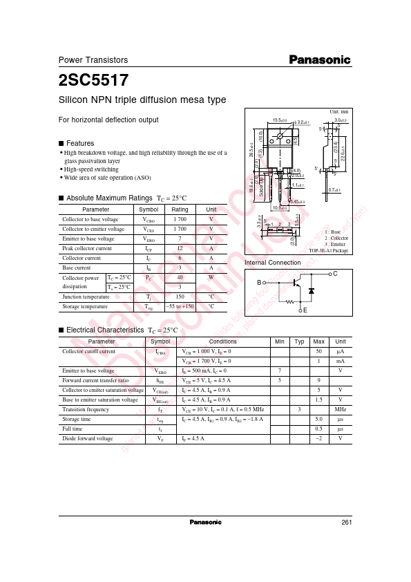
FEATURES
● High breakdown voltage, and high reliability through the use of a glass passivation layer● High-speed switching
● Wide area of safe operation (ASO) 5˚ (4.0) 5˚ 2.0±0.2 5˚ / 1.1±0.1 0.7±0.1 I
ABSOLUTE MAXIMUM RATINGS
TC = 25°C 5.45±0.3 e ) Parameter Symbol Rating Unit 18.6±0.5 (2.0) Solder Dip c type Collector to base voltage VCBO 1 700 V 3.3±0.3 5.5±0.3 n d ge. ed Collector to emitter voltage VCES 1 700 (2.0) V sta tinu Emitter to base voltage VEBO 7 V a e cle con Peak collector current ICP 12 A lifecy , dis Collector current IC 6 A n u ct ed Base current IB 3 A du typ Collector power TC = 25°C PC 40 W te tin Pro ued dissipation Ta = 25°C 3 four ntin Junction temperature Tj 150 °C wing disco Storage temperature Tstg −55 to +150 °C 10.9±0.5 5˚ 12 3 1 : Base 2 : Collector 3 : Emitter TOP-3E-A1 Package Internal Connection C B E in ndes foll,oplaned IELECTRICAL CHARACTERISTICS
TC = 25°C a o inclu type Parameter Symbol Conditions Min Typ Max Unit c ed ce Collector cutoff curren...