2SK3559
Overview
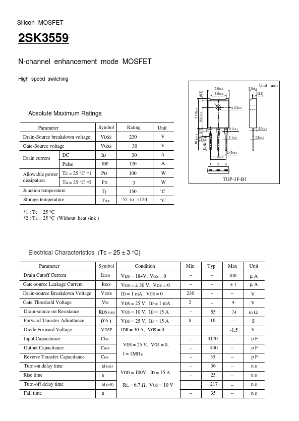
Silicon MOSFET 2SK3559 N-channel enhancement mode MOSFET High speed switching Absolute Maximum Ratings Parameter Drain-Source breakdown voltage Gate-Source voltage Drain current DC Pulse Allowa...
Silicon MOSFET 2SK3559 N-channel enhancement mode MOSFET High speed switching Absolute Maximum Ratings Parameter Drain-Source breakdown voltage Gate-Source voltage Drain current DC Pulse Allowa...
| Part Number | Manufacturer | Description |
|---|---|---|
| 2SK3555-01MR | Inchange Semiconductor | N-Channel MOSFET Transistor |
| 2SK3556-01L | Inchange Semiconductor | N-Channel MOSFET Transistor |
| 2SK3556-01S | Inchange Semiconductor | N-Channel MOSFET Transistor |