Overview: Switching Diodes MA3S132A
Silicon epitaxial planar type
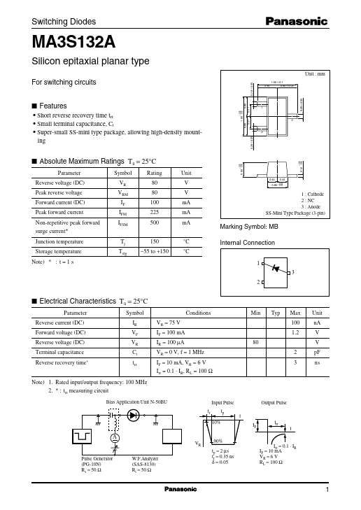
Unit : mm
0.28 ± 0.05 For switching circuits
1.60 − 0.03 0.80 0.80 0.51 0.51 1.60 ± 0.1 0.80 0.80 ± 0.05 Parameter Reverse voltage (DC) Peak reverse voltage Forward current (DC) Peak forward current Non-repetitive peak forward surge current* Junction temperature Storage temperature Note) * : t = 1 s Symbol VR VRM IF IFM IFSM Tj Tstg Rating 80 80 100 225 500 150 −55 to +150 Unit V V mA mA mA °C °C 0.60 − 0.03 0.44 0.44
+ 0.05 0.88 − 0.03 1 : Cathode 2 : NC 3 : Anode SS-Mini Type Package (3-pin) Marking Symbol: MB Internal Connection
1 3 2 
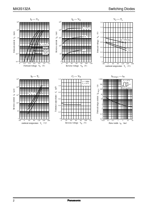
I Electrical Characteristics Ta = 25°C
Parameter Reverse current (DC) Forward voltage (DC) Reverse voltage (DC) Terminal capacitance Reverse recovery time* Symbol IR VF VR Ct trr VR = 75 V IF = 100 mA IR = 100 µA VR = 0 V, f = 1 MHz IF = 10 mA, VR = 6 V Irr = 0.1 · IR, RL = 100 Ω 80 2 3 Conditions Min Typ Max 100 1.2 Unit nA V V pF ns Note) 1. Rated input/output frequency: 100 MHz 2. * : trr measuring circuit
Bias Application Unit N-50BU tr 10% Input Pulse tp t IF trr t Irr = 0.1 · IR IF = 10 mA VR = 6 V RL = 100 Ω Output Pulse A
VR Pulse Generator (PG-10N) Rs = 50 Ω W.F.Analyzer (SAS-8130) Ri = 50 Ω 90% tp = 2 µs tr = 0.35 ns δ = 0.05 0.12 − 0.02 + 0.05 + 0.05 I Absolute Maximum Ratings Ta = 25°C 0.28 ± 0.05 • Short reverse recovery time trr • Small terminal capacitance, Ct • Super-small SS-mini type package, allowing high-density mounting + 0.