Datasheet4U Logo Datasheet4U.com

MN31121SA - CCD Image Sensor Vertical Driver IC

Description

Pin No.

1 2 3 4 5 6 7 8 9 10 11 12 13 14 15 16 17 18 19 20 Pin name OSUB VL OV2 VM13 OV1 VDC IV1 CH1 IV2 ISUB N.C.

IV4 CH2 IV3 N.C.

Features

  • s.
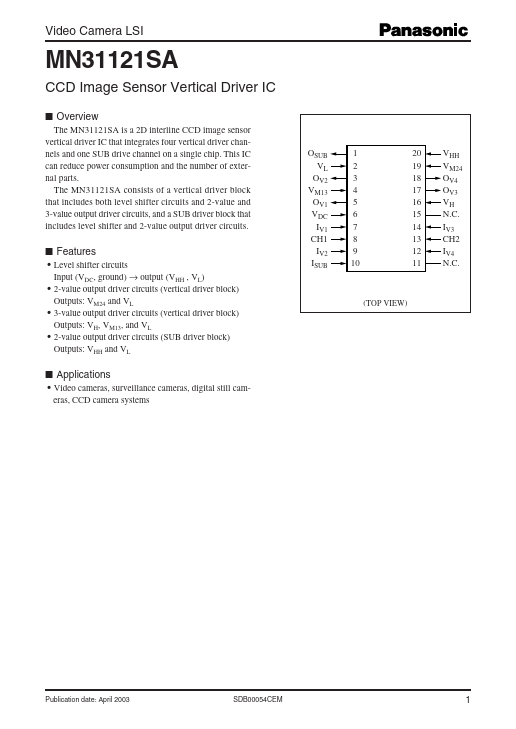
  • Level shifter circuits Input (VDC, ground) → output (VHH , VL).
  • 2-value output driver circuits (vertical driver block) Outputs: VM24 and VL.
  • 3-value output driver circuits (vertical driver block) Outputs: VH, VM13, and VL.
  • 2-value output driver circuits (SUB driver block) Outputs: VHH and VL OSUB VL OV2 VM13 OV1 VDC IV1 CH1 IV2 ISUB 1 2 3 4 5 6 7 8 9 10 20 19 18 17 16 15 14 13 12 11 VHH VM24 OV4 OV3 VH N. C. IV3 CH2 IV4 N. C. (TOP VIEW).
  • Applicatio.

📥 Download Datasheet

Datasheet preview – MN31121SA

Datasheet Details

Part number MN31121SA
Manufacturer Panasonic
File Size 173.27 KB
Description CCD Image Sensor Vertical Driver IC
Datasheet download datasheet MN31121SA Datasheet
Additional preview pages of the MN31121SA datasheet.
Other Datasheets by Panasonic

Full PDF Text Transcription

Click to expand full text
Video Camera LSI MN31121SA CCD Image Sensor Vertical Driver IC ■ Overview The MN31121SA is a 2D interline CCD image sensor vertical driver IC that integrates four vertical driver channels and one SUB drive channel on a single chip. This IC can reduce power consumption and the number of external parts. The MN31121SA consists of a vertical driver block that includes both level shifter circuits and 2-value and 3-value output driver circuits, and a SUB driver block that includes level shifter and 2-value output driver circuits.
Published: |