FEATURES
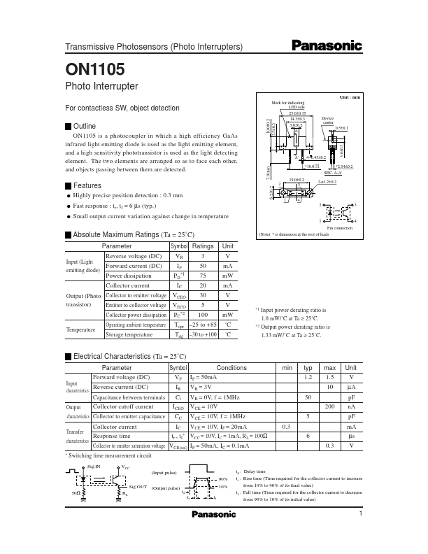
2 19.0±0.2 3 1 4 2 3 ,,, , *2.54±0.2 SEC. A-A' 2-ø3.2±0.2 1 3.0±0.2 4 ABSOLUTE MAXIMUM RATINGS
(Ta = 25˚C) Parameter Reverse voltage (DC) Input (Light Forward current (DC) emitting diode) Power dissipation Collector current Symbol Ratings VR IF PD*1 IC 3 50 75 20 30 5 100 Unit V mA mW mA V V mW ˚C ˚C Pin connection (Note) * is dimension at the root of leads Output (Photo Collector to emitter voltage VCEO transistor) Emitter to collector voltage VECO Collector power dissipation Temperature Operating ambient temperature Storage temperature PC*2 *1 Topr –25 to +85 Tstg –30 to +100 Input power derating ratio is 1.0 mW/˚C at Ta ≥ 25˚C. *2 Output power derating ratio is 1.33 mW/˚C at Ta ≥ 25˚C. ELECTRICAL CHARACTERISTICS
(Ta = 25˚C) Parameter Forward voltage (DC) Input Reverse current (DC) characteristics Capacitance between terminals Collector cutoff current Output characteristics Collector to emitter capacitance Symbol VF IR Ct ICEO CC VR = 3V VR = 0V, f = 1MHz VCE = 10V VCE = 10V... Panasonic