Panasonic XN1871
Silicon N-channel junction FET
| Part No. | XN1871 |
|---|---|
| Datasheet | XN1871 Download |
| Manufacturer |  Panasonic |
| Description | Silicon N-channel junction FET |
| Buy | Stock & Price |
ABSOLUTE MAXIMUM RATINGS
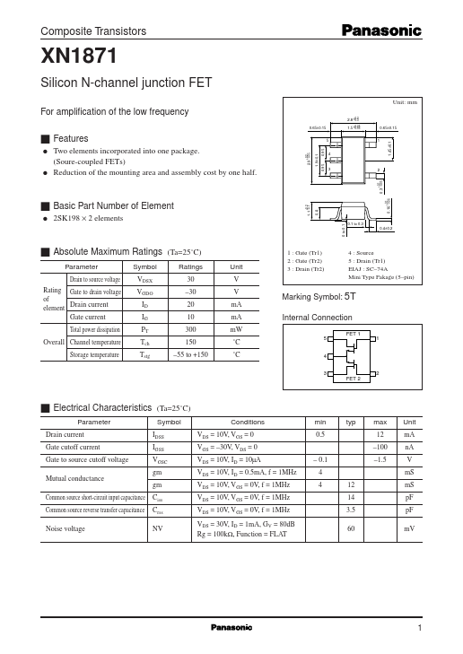
Parameter Drain to source voltage Rating Gate to drain voltage of Drain current element Gate current Total power dissipation Overall Channel temperature Storage temperature Symbol VDSX VGDO ID IG PT Tch Tstg (Ta=25˚C) Ratings 30 –30 20 10 300 150 –55 to +150 Unit V V mA mA mW ˚C ˚C 1 : Gate (Tr1) 2 : Gate (Tr2) 3 : Drain (Tr2) 0 to 0.1 0.1 to 0.3 4 : Source 5 : Drain (Tr1) EIAJ : SC–74A Mini Type Pakage (5–pin) Marking Symbol: 5T Internal Connection 5 4 3 2 FET 1 1 FET 2 sELECTRICAL CHARACTERISTICS
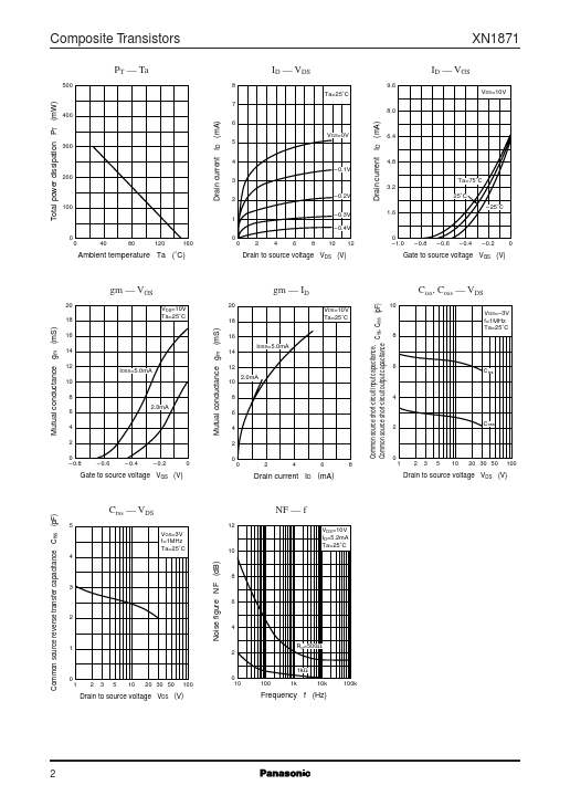
Parameter Drain current Gate cutoff current Gate to source cutoff voltage Mutual conductance Common source short-circuit input capacitance Common source reverse transfer capacitance Noise voltage (Ta=25˚C) Symbol IDSS IGSS VGSC gm gm Ciss Crss NV Conditions VDS = 10V, VGS = 0 VGS = –30V, VDS = 0 VDS = 10V, ID = 10µA VDS = 10V, ID = 0.5mA, f = 1MHz VDS = 10V, VGS = 0V, f = 1MHz VDS = 10V, VGS = 0V, f = 1MHz VDS = 10V, VGS = 0V, f = 1MHz VDS = 30V, ID = 1mA, GV = 80dB...