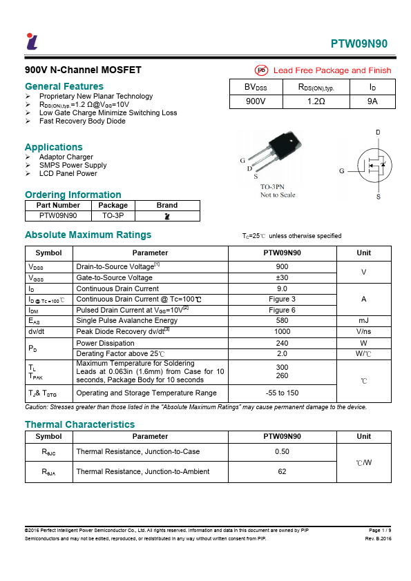
Proprietary New Planar Technology RDS(ON),typ. =1.2 Ω@VGS=10V Low Gate Charge Minimize Switching Loss Fast Recovery Body Diode
PTW09N90
BVDSS
RDS(ON),typ. ID
900V
1.2Ω
9A.
Full PDF Text Transcription for PTW09N90 (Reference)
Note: Below is a high-fidelity text extraction (approx. 800 characters) for
PTW09N90. For precise diagrams, and layout, please refer to the original PDF.
900V N-Channel MOSFET General Features Proprietary New Planar Technology RDS(ON),typ.=1.2 Ω@VGS=10V Low Gate Charge Minimize Switching Loss Fast Recovery Body Diode PTW09...
View more extracted text
Low Gate Charge Minimize Switching Loss Fast Recovery Body Diode PTW09N90 BVDSS RDS(ON),typ. ID 900V 1.2Ω 9A Applications Adaptor Charger SMPS Power Supply LCD Panel Power Ordering Information Part Number Package PTW09N90 TO-3P Brand Absolute Maximum Ratings ℃ TC=25 unless otherwise specified Symbol VDSS VGSS ID ℃ ID @ Tc =100 IDM EAS dv/dt PD TL TPAK Parameter Drain-to-Source Voltage[1] Gate-to-Source Voltage Continuous Drain Current ℃ Continuous Drain Current @ Tc=100 Pulsed Drain Current at VGS=10V[2] Single Pulse Avalanche Energy Peak Diode Recovery dv/dt[3] Power Dissipation ℃ Derating Factor above 25 Maximum Temperat