Datasheet4U Logo Datasheet4U.com

PI90LVT211 - 1:6 Differential Clock Distribution Chip

General Description

The PI90LV211 implements low voltage differential signaling (LVDS) to achieve clocking rates as high as 320 MHz with low skew.

The PI90LV211 is a low skew 1:6 fanout device designed explicitly for low skew clock distribution applications.

Key Features

  • Meets or Exceeds Requirements of ANSI TIA/EIA-644-1995 Designed for Clocking Rates up to 320MHz Operates from a single 3.3-V Supply Low-Voltage Differential Signaling (LVDS) with Output Voltages of ±350mV into a 100-ohm load Choice between LVDS or TTL clock input Synchronous Enable/Disable Multiplexed clock input.
  • Internal 300 kohm pullup resistor on all control pins.
  • CLK and CLK have 110-ohm termination (PI9.

📥 Download Datasheet

Full PDF Text Transcription (Reference)

The following content is an automatically extracted verbatim text from the original manufacturer datasheet and is provided for reference purposes only.

View original datasheet text
12345678901234567890123456789012123456789012345678901234567890121234567890123456789012345678901212345678901234567890123456789012123456789012 12345678901234567890123456789012123456789012345678901234567890121234567890123456789012345678901212345678901234567890123456789012123456789012 
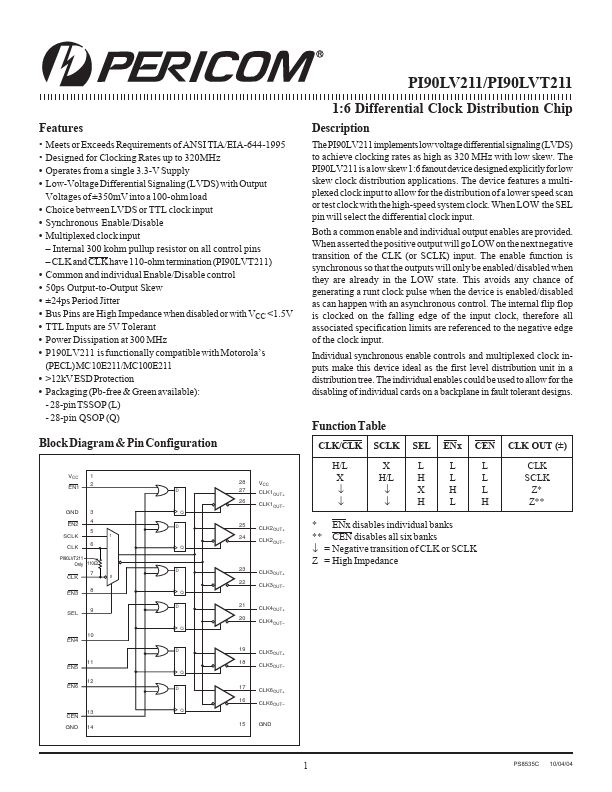
PI90LV211/PI90LVT211 1:6 Differential Clock Distribution Chip Features • • • • • • • Meets or Exceeds Requirements of ANSI TIA/EIA-644-1995 Designed for Clocking Rates up to 320MHz Operates from a single 3.