Datasheet Summary
4-Output Low Power PCIE GEN1-2-3 Buffer
Features
ÎÎ4x 100MHz low power HCSL or LVDS patible outputs ÎÎPCIe 3.0, 2.0 and 1.0 pliant ÎÎProgrammable output amplitude and slew rate ÎÎCore supply voltage of 3.3V +/-10% ÎÎOutput supply voltage of 1.8V, 2.5V and 3.3V ÎÎIndustrial ambient operation temperature ÎÎAvailable in lead-free package: 32-TQFN
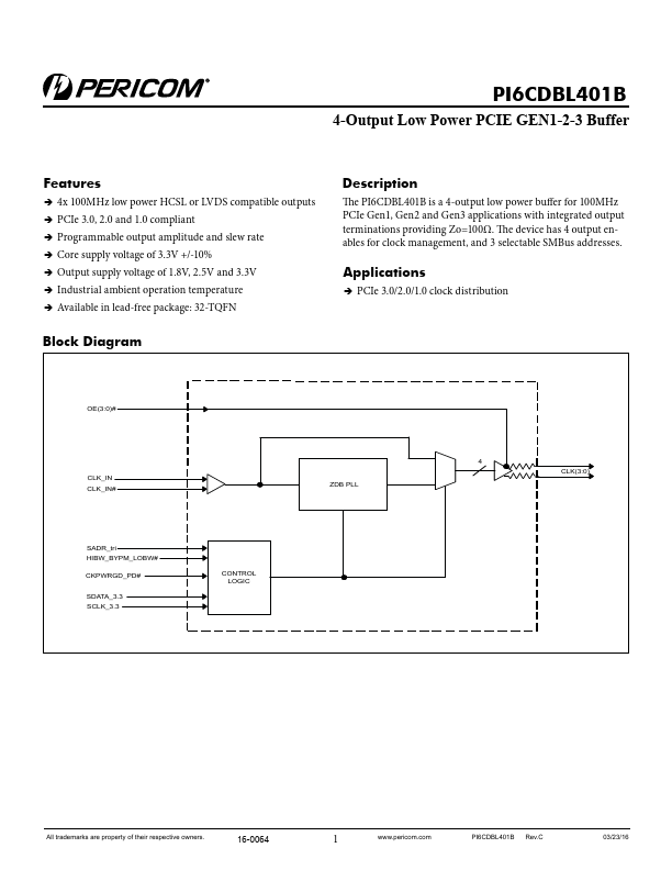
Block Diagram
Description
The PI6CDBL401B is a 4-output low power buffer for 100MHz PCIe Gen1, Gen2 and Gen3 applications with integrated output terminations providing Zo=100Ω. The device has 4 output enables for clock management, and 3 selectable SMBus addresses.
Applications
ÎÎPCIe 3.0/2.0/1.0 clock distribution
OE(3:0)#
CLK_IN...