PI90LVB16
PI90LVB16 is 3V Bus LVDS 1-to-6 Clock Buffer/Bus Transceiver manufactured by Pericom Semiconductor.
Features
Master/Slave clock selection in a backplane application 160 MHz operation (typical) 100ps duty cycle distortion (typical) 50ps channel to channel skew (typical) 3.3V power supply design Glitch-free power on at CLKI/O pins Low Power design (16m A @ 3.3V static) Accepts small swing (300m V typical) differential signal levels Industrial temperature operating range (40°C to +85°C) Available in 24-pin TSSOP Packaging (L)
General Description
3V Bus LVDS 1-to-6 Clock Buffer/Bus Transceiver
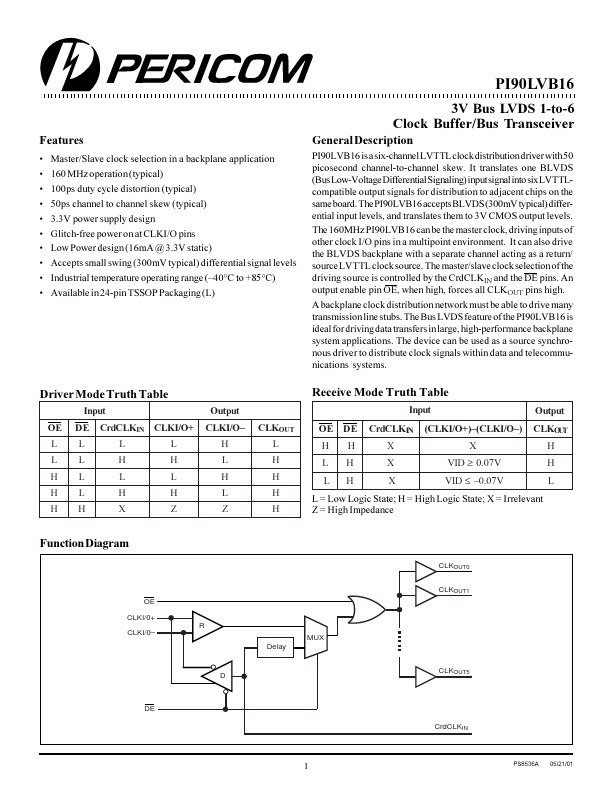
PI90LVB16 is a six-channel LVTTL clock distribution driver with 50 picosecond channel-to-channel skew. It translates one BLVDS (Bus Low-Voltage Differential Signaling) input signal into six LVTTLpatible output signals for distribution to adjacent chips on the same board. The PI90LVB16 accepts BLVDS (300m V typical) differential input levels, and translates them to 3V CMOS output levels. The 160MHz PI90LVB16 can be the master clock, driving inputs of other clock I/O pins in a multipoint environment. It can also drive the BLVDS backplane with a separate channel acting as a return/ source LVTTL clock source. The master/slave clock selection of the driving source is controlled by the Crd CLKIN and the DE pins. An output enable pin OE, when high, forces all CLKOUT pins high. A backplane clock distribution network must be able to drive many transmission line stubs. The Bus LVDS feature of the PI90LVB16 is ideal for driving data transfers in large, high-performance backplane system applications. The device can be used as a source synchronous driver to distribute clock signals within data and telemunications systems.
Driver Mode Truth Table
Input OE L L H H H DE L L L L H Crd CLKIN CLKI/O+ L H L H X L H L H Z Output CLKI/O H L H L Z CLKOUT L H H H H
Receive Mode Truth Table
Input OE DE H L L H H H Crd CLKIN X X X (CLKI/O+)(CLKI/O) X VID ≥ 0.07V VID ≤ 0.07V Output CLKOUT H H L
L = Low Logic State; H = High Logic State; X = Irrelevant Z = High Impedance
Function...