FEATURES
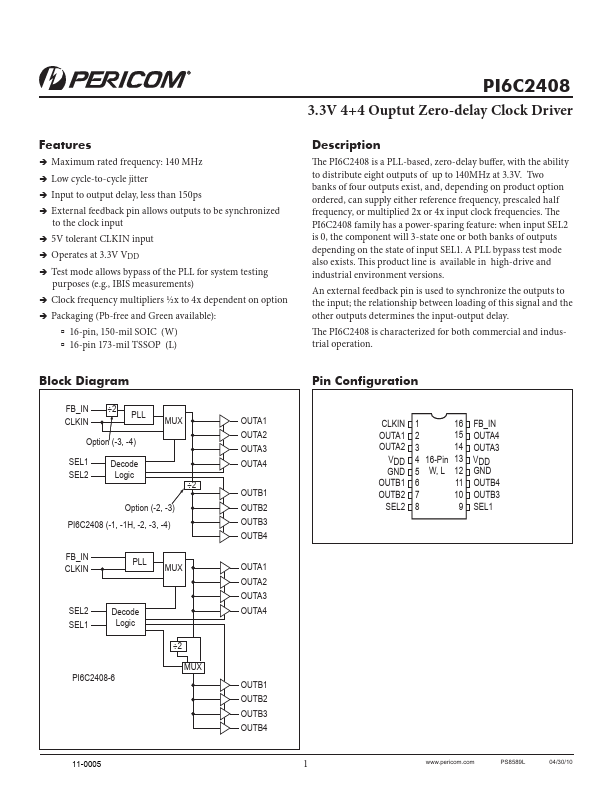
ÎÎMaximum rated frequency: 140 MHz ÎÎLow cycle-to-cycle jitter ÎÎInput to output delay, less than 150ps ÎÎExternal feedback pin allows outputs to be synchronized to the clock input ÎÎ5V tolerant CLKIN input ÎÎOperates at 3.3V VDD ÎÎTest mode allows bypass of the PLL for system testing purposes (e.g., IBIS measurements) ÎÎClock frequency multipliers ½x to 4x dependent on option ÎÎPackaging (Pb-free and Green available): àà 16-pin, 150-mil SOIC (W) àà 16-pin 173-mil TSSOP (L) DESCRIPTION
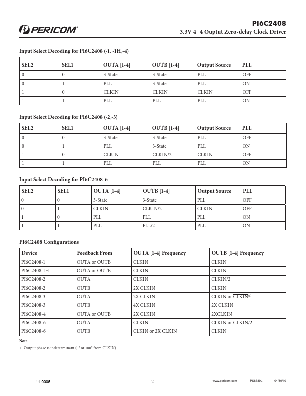
Two banks of four outputs exist, and, depending on product option ordered, can supply either reference frequency, prescaled half frequency, or multiplied 2x or 4x input clock frequencies. Pericom Semiconductor