Pericom Semiconductor PI6C2409
The PI6C2409 is a PLL based, zero-delay buffer, with the ability to distribute nine outputs of up to 133MHz at 3.3V. It also has a powersparing feature: when input SEL1 is 0 and SEL2 is 1, PLL is turned off and all outputs are referenced from CLKIN. PI6C2409 is available in high drive and industrial environment versions.| Part No. | PI6C2409 |
|---|---|
| Datasheet | PI6C2409 Download |
| Manufacturer |  Pericom Semiconductor |
| Description | Zero-Delay Clock Buffer |
| Buy | Stock & Price |
FEATURES
●●
●
● Maximum rated frequency: 133 MHz Low cycle-to-cycle jitter Input to output delay, less than 200ps Internal feedback allows outputs to be synchronized to the clock input
● Operates at 3.3V VDD
● Space-saving Packages: 150-mil SOIC (W) 173-mil TSSOP (L) Functional
DESCRIPTION
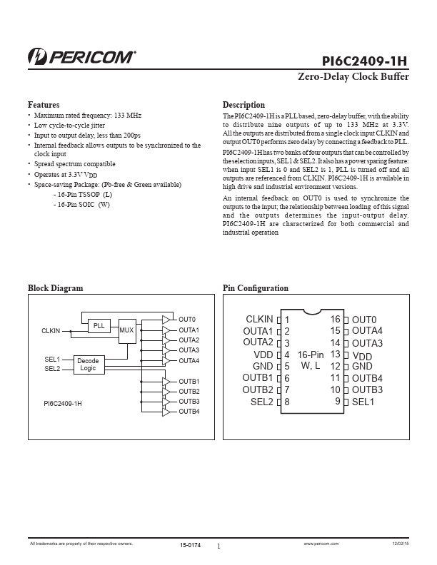
All the outputs are distributed from a single clock input CLKIN and output OUT0 performs zero delay by connecting a feedback to PLL. PI6C2409 has two banks of four outputs that can be controlled by the selection inputs, SEL1 & SEL2. An internal feedback on OUT0 is used to synchronize the outputs to the input; the relationship between loading of this signal and the outputs determines the input-output delay. PI6C2409 are characterized for both commercial and industrial operation Block Diagram OUT0 CLKIN PLL MUX OUTA1 OUTA2 OUTA3 SEL1 SEL2 Decode Logic OUTA4 OUTB1 OUTB2 PI6C2409(-1, -1H) OUTB3 OUTB4 Pin Configuration CLKIN OUTA1 OUTA2 VDD GND OUTB1 OUTB2 SEL2 1 2 3 4 5 6 7 8 16 15 16-Pin 14 W, L 13 12...
