PLL102-10
PLL102-10 is Low Skew Output Buffer manufactured by PhaseLink Corporation.
FEATURES
Frequency range 50 ~ 120MHz. Internal phase locked loop will allow spread spectrum modulation on reference clock to pass to outputs.
- Zero input
- output delay.
- Less than 700 ps device
- device skew.
- Less than 250 ps skew between outputs. ..
- Less than 100 ps cycle
- cycle jitter.
- 2.5V or 3.3V power supply operation.
- Available in 8-Pin SOIC or MSOP package.
- -
PIN CONFIGURATION
REFIN GND CLK1 CLK2
CLKOUT DNC DNC VDD
2 3 4
7 6 5
DESCRIPTION
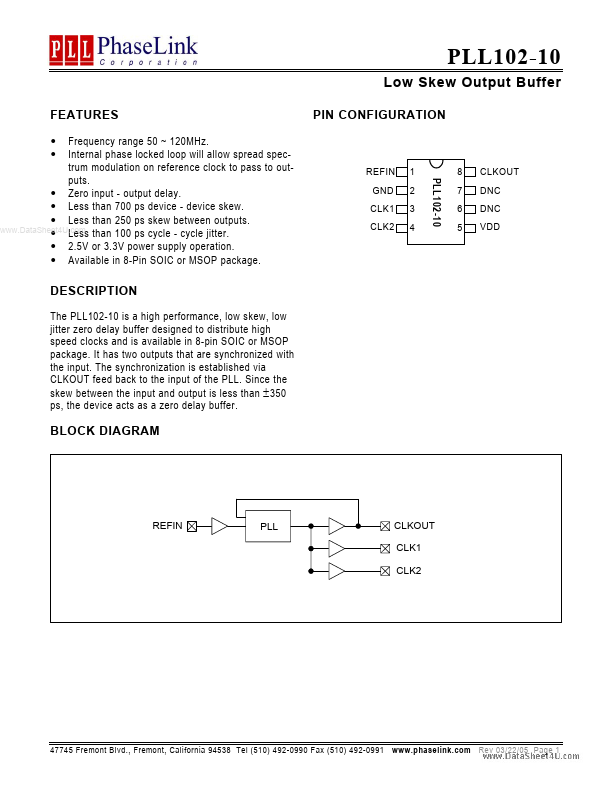
The PLL102-10 is a high performance, low skew, low jitter zero delay buffer designed to distribute high speed clocks and is available in 8-pin SOIC or MSOP package. It has two outputs that are synchronized with the input. The synchronization is established via CLKOUT feed back to the input of the PLL. Since the skew between the input and output is less than ± 350 ps, the device acts as a zero delay buffer.
BLOCK DIAGRAM
REFIN
CLKOUT CLK1 CLK2
47745 Fremont Blvd., Fremont, California 94538 Tel (510) 492-0990 Fax (510) 492-0991 .phaselink. Rev 03/22/05 Page 1
Low Skew Output Buffer
PIN DESCRIPTIONS
Name
REFIN GND CLK1 CLK2 VDD .. DNC CLKOUT2
Number
1 2 3 4 5 6&7 8
Type
I P O O P O
Description
Input reference frequency. Spread spectrum modulation on this signal will be passed to the output (up to 100k Hz SST modulation). Ground Connection. Buffered clock output. Buffered clock output. 2.5V or 3.3V Power Supply connection. Do Not Connect Buffered clock output. Internal feed back on this pin.
ELECTRICAL SPECIFICATIONS
1. Absolute Maximum Ratings PARAMETERS
Supply Voltage Input Voltage, dc Output Voltage, dc Storage Temperature Ambient Operating Temperature- Junction Temperature Lead Temperature (soldering,...