PJM2300NSA Overview
Key Features
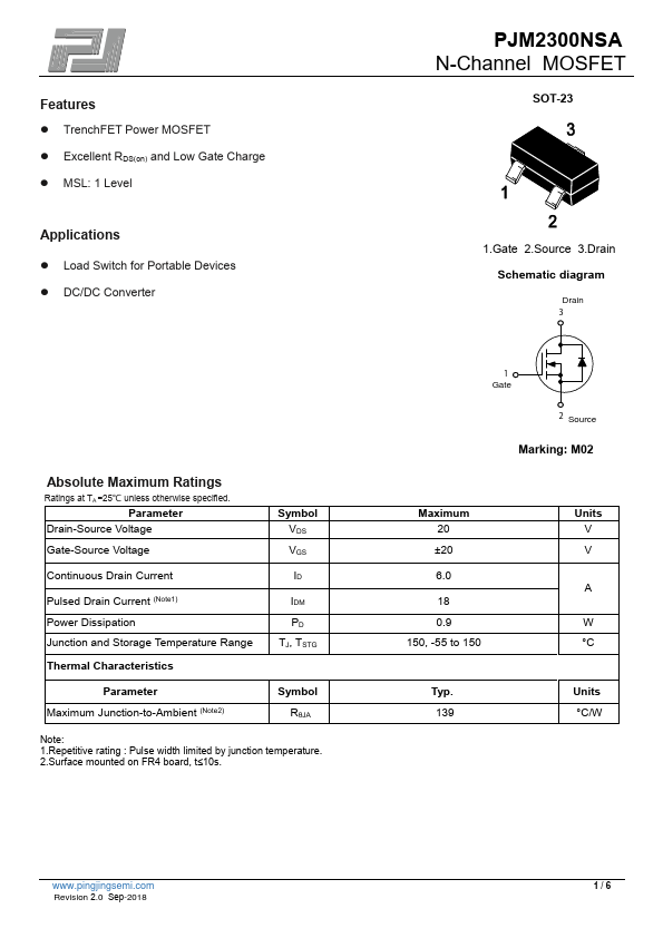
- TrenchFET Power MOSFET
- Excellent RDS(on) and Low Gate Charge
- MSL: 1 Level
| Part | PJM2300NSA |
|---|---|
| Description | N-Channel MOSFET |
| Category | MOSFET |
| Manufacturer | Ping Jing |
| Size | 1.49 MB |
| Seller | Inventory | Price Breaks | Buy |
|---|---|---|---|
| LCSC | 3000 | 10+ : 0.0466 USD 100+ : 0.037 USD 300+ : 0.0323 USD 3000+ : 0.0255 USD |
View Offer |
| Axis Part Limited | 3200 | 10+ : 0.0442 USD 100+ : 0.0351 USD 300+ : 0.0305 USD 3000+ : 0.0241 USD |
View Offer |
| Part Number | Manufacturer | Description |
|---|---|---|
| AP9563GH | Advanced Power Electronics Corp | P-CHANNEL ENHANCEMENT MODE POWER MOSFET |
| A2SHB | HAOHAI | N-Channel MOSFET |
| FCPF360N65S3R0L | onsemi | N-Channel MOSFET |