Potens semiconductor PDP0903
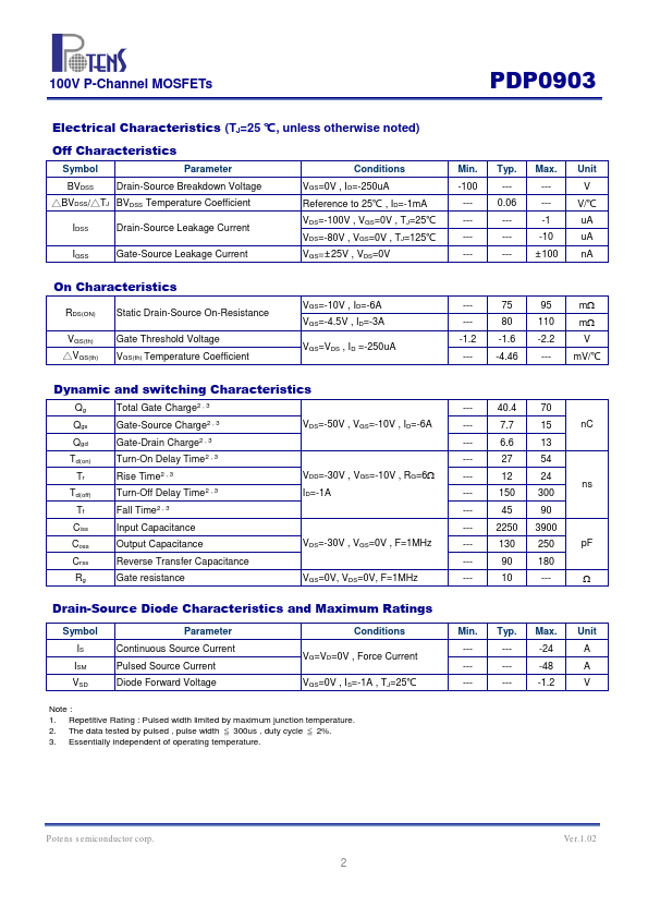
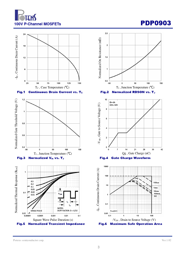
This advanced technology has been especially tailored to minimize on-state resistance, provide superior switching performance, and withstand high energy pulse in the avalanche and commutation mode. These devices are well suited for high efficiency fast switching applications.| Part No. | PDP0903 |
|---|---|
| Datasheet | PDP0903 Download |
| Manufacturer |  Potens semiconductor |
| Description | P-Channel MOSFETs |
| Buy | Stock & Price |
GENERAL DESCRIPTION
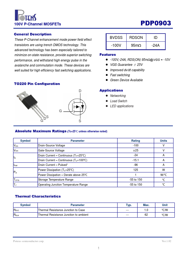
These P-Channel enhancement mode power field effect transistors are using trench DMOS technology. TO220 Pin Configuration D G GDS S BVDSS -100V RDSON 95m ID -24AFEATURES
● -100V,-24A, RDS(ON) 95mΩ@VGS = -10V● VGS Guarantee ± 25V
● Improved dv/dt capability
● Fast switching
● Green Device Available
APPLICATIONS
● Networking● Load Switch
● LED applications
ABSOLUTE MAXIMUM RATINGS
(Tc=25℃ unless otherwise noted) Symbol VDS VGS ID IDM PD TSTG TJ Parameter Drain-Source Voltage Gate-Source Voltage Drain Current – Continuous (TC=25℃) Drain Current – Continuous (TC=100℃) Drain Current – Pulsed1 Power Dissipation (TC=25℃) Power Dissipation – Derate above 25℃ Storage Temperature Range Operating Junction Temperature Range Rating -100 ±25 -24 -15.1 -96 125 1 -55 to 150 -55 to 150 Units V V A A A W W/℃ ℃ ℃ Thermal Characteristics Symbol RθJC RθJA Parameter Thermal Resistance Junction to Case Thermal Resistance Junction to ambient Typ. ----- Max. 1.0 62 Unit ℃/W ℃/W Potens semiconductor corp.