PPM723T201E0 Overview
Description
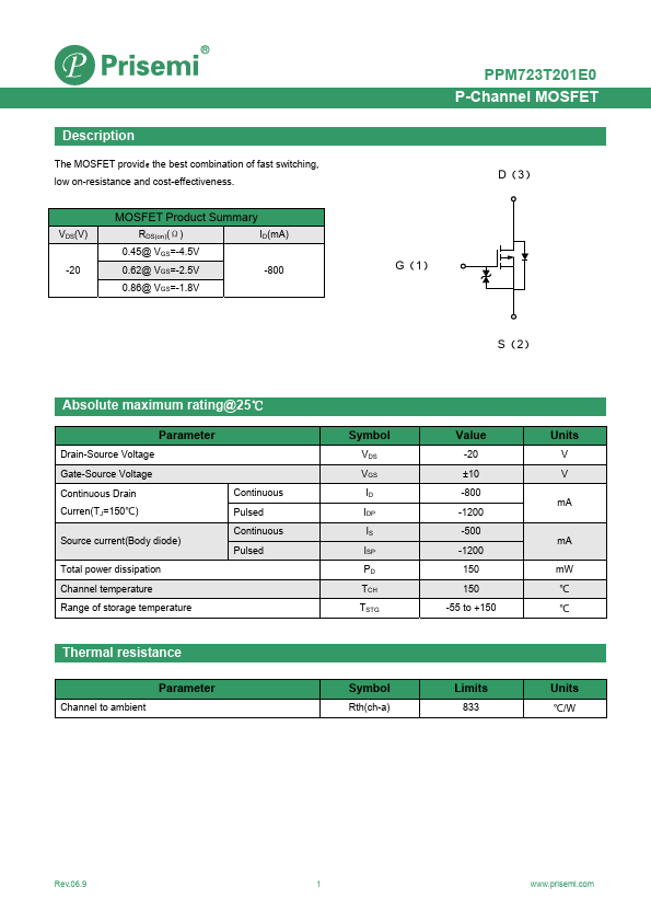
The MOSFET provide the best combination of fast switching, low on-resistance and cost-effectiveness. VDS(V) -20 MOSFET Product Summary RDS(on)(Ω) ID(mA) 0.45@ VGS=-4.5V 0.62@ VGS=-2.5V -800 0.86@ VGS=-1.8V PPM723T201E0 P-Channel MOSFET D(3) G(1) S(2) Absolute maximum rating@25℃ Parameter Drain-Source Voltage Gate-Source Voltage Continuous Drain Curren(TJ=150℃) Source current(Body diode) Total power dissipation Channel temperature Range of storage temperature Continuous Pulsed Continuous Pulsed Parameter Channel to ambient Symbol VDS VGS ID IDP IS ISP PD TCH TSTG Value -20 ±10 -800 -1200 -500 -1200 150 150 -55 to +150 Units V V mA mA mW ℃ ℃ Symbol Rth(ch-a) Limits 833 Units ℃/W Rev.06.9 1 P-Channel MOSFET PPM723T201E0 Parameter Drain-Source Breakdown Voltage Zero Gate Voltage Drain Current Gate-Body Leakage Current Gate Threshold Voltage Static Drain-Source On-Resistance Forward transfer admittance Input Capacitance Output Capacitance Reverse Transfer Capacitance Turn-On Delay Time Turn-Off Delay Time Turn-On Rise Time Turn-On Fall Time Total Gate Charge Gate-Source Charge Gate-Drain Charge Drain-Source Diode Forward Voltage Symbol BVDSS IDSS IGSS VGS(th) RDS(ON) ︱Yfs︱ CISS COSS CRSS td(on) td(off) tr tf Qg Qgs Qgd VSD Conditions ID =-1mA,VGS=0V VDS =-20V,VGS=0V VDS =0V,VGS=±8V VDS =-10V, ID =-100μA VGS=-4.5V, ID =-700mA VGS=-2.5V, ID =-300mA VGS=-1.8V, ID =-250mA VDS=-10V, ID =-200mA VGS=0V, VDS =-10V, f=1MHz VDD≒-10V, VGS =-4.5V, RG=10Ω,RL≒100Ω ID =-100mA VDD≒-10V , VGS =-4.5V, ID =-200mA RG=10Ω,RL≒50Ω VGS=0V,IS=-200mA Min.