PPM8PN30V12 Overview
Description
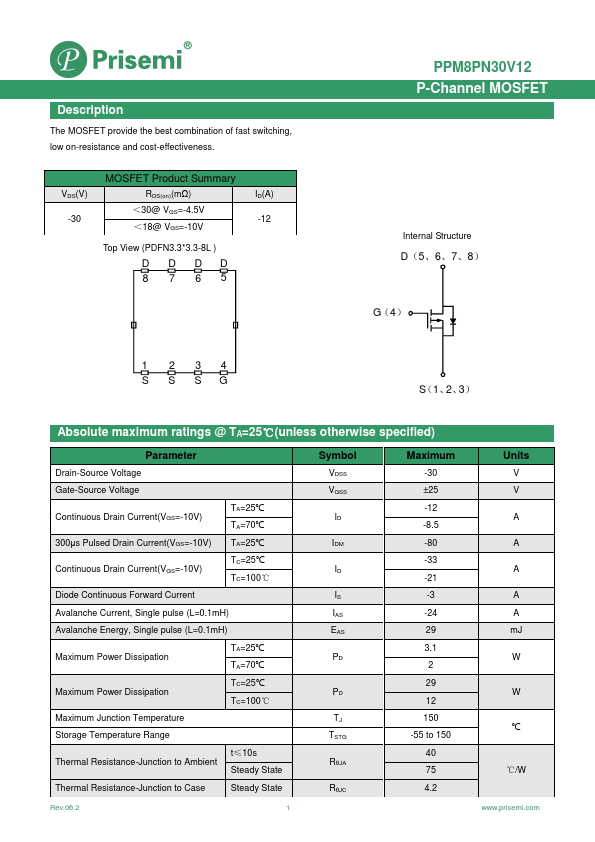
The MOSFET provide the best combination of fast switching, low on-resistance and cost-effectiveness. VDS(V) -30 MOSFET Product Summary RDS(on)(mΩ) <30@ VGS=-4.5V <18@ VGS=-10V Top View (PDFN3.3*3.3-8L ) D D DD 8765 ID(A) -12 PPM8PN30V12 P-Channel MOSFET Internal Structure D(5、6、7、8) G(4) 1 234 S S SG S(1、2、3) Parameter Drain-Source Voltage Gate-Source Voltage Continuous Drain Current(VGS=-10V) 300μs Pulsed Drain Current(VGS=-10V) TA=25℃ TA=70℃ TA=25℃ Continuous Drain Current(VGS=-10V) TC=25℃ TC=100℃ Diode Continuous Forward Current Avalanche Current, Single pulse (L=0.1mH) Avalanche Energy, Single pulse (L=0.1mH) Maximum Power Dissipation TA=25℃ TA=70℃ Maximum Power Dissipation TC=25℃ TC=100℃ Maximum Junction Temperature Storage Temperature Range t≤10s Steady State Steady State Symbol VDSS VGSS ID IDM ID IS IAS EAS PD PD TJ TSTG RθJA RθJC Maximum -30 ±25 -12 -8.5 -80 -33 -21 -3 -24 29 3.1 2 29 12 150 -55 to 150 40 75 4.2 Rev.06.2 1 Units V V A A A A A mJ W W ℃ ℃/W P-Channel MOSFET PPM8PN30V12 Parameter Drain-Source Breakdown Voltage Zero Gate Voltage Drain Current Gate-Body Leakage Current Gate Threshold Voltage Static Drain-Source On-Resistance Drain-Source Diode Forward Voltage Reverse Recovery Time Reverse Recovery Charge Total Gate Charge Gate-Source Charge Gate-Drain Charge Input Capacitance Output Capacitance Reverse Transfer Capacitance Turn-On Delay Time Turn-Off Delay Time Turn-On Rise Time Turn-On Fall Time Gate Resistance Symbol BVDSS IDSS IGSS VGS(th) RDS(ON) VSD trr Qrr Qg Qgs Qgd Ciss Coss Crss td(on) td(off) tr tf Rg Conditions IDS=-250μA, VGS=0V VDS=-24V, VGS=0V TJ=85℃ VDS=0V, VGS=±20V VDS=VGS, IDS=-250μA VGS=-10V, IDS=.