PPMS8N20V3 Overview
Description
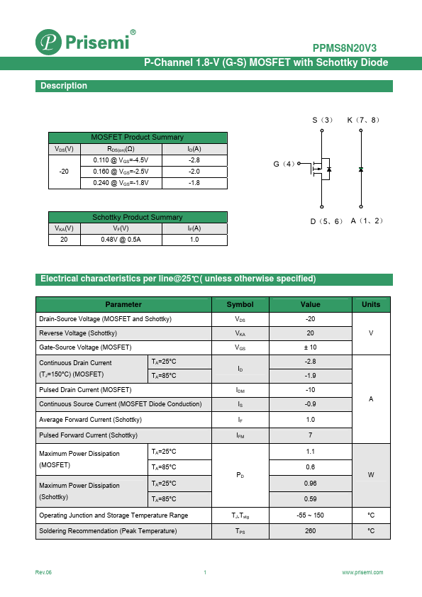
PPMS8N20V3 P-Channel 1.8-V (G-S) MOSFET with Schottky Diode VDS(V) -20 MOSFET Product Summary RDS(on)(Ω) ID(A) 0.110 @ VGS=-4.5V -2.8 0.160 @ VGS=-2.5V -2.0 0.240 @ VGS=-1.8V -1.8 S(3) K(7、8) G(4) VKA(V) 20 Schottky Product Summary VF(V) IF(A) 0.48V @ 0.5A 1.0 D(5、6) A(1、2) Parameter Drain-Source Voltage (MOSFET and Schottky) Reverse Voltage (Schottky) Gate-Source Voltage (MOSFET) Continuous Drain Current (TJ=150°C) (MOSFET) TA=25°C TA=85°C Pulsed Drain Current (MOSFET) Continuous Source Current (MOSFET Diode Conduction) Average Forward Current (Schottky) Pulsed Forward Current (Schottky) Maximum Power Dissipation (MOSFET) TA=25°C TA=85°C Maximum Power Dissipation (Schottky) TA=25°C TA=85°C Operating Junction and Storage Temperature Range Soldering Recommendation (Peak Temperature) Symbol VDS VKA VGS ID IDM IS IF IFM PD TJ,Tstg TPS Value -20 20 ± 10 -2.8 -1.9 -10 -0.9 1.0 7 1.1 0.6 0.96 0.59 -55 ~ 150 260 Units V A W °C °C Rev.06 1 MOSFET with Schottky Parameter MOSFET Schottky MOSFET Schottky MOSFET Schottky PPMS8N20V3 Condition t ≤ 5sec Steady State Steady State Symbol RthJA RthJP Typical 50 77 90 110 30 33 Maximum 60 95 110 130 40 40 Unit °C/W MOSFET Specifications (TJ=25℃ Unless Otherwise Noted) Parameter Static Gate Threshold Voltage Gate-Body Leakage Current Zero Gate Voltage Drain Current On-State Drain Current Symbol VGS(th) IGSS IDSS ID(on) Drain-Source On-State Resistance RDS(on) Forward Tran Conductance Diode Forward Voltage Dynamic Total Gate Charge Gate-Source Charge Gate-Drain Charge Turn-On Delay Time Rise Time Turn-Off Delay Time Fall Time Source-Drain Reverse Recovery Time gfs VSD Qg Qgs Qgd td(on) tr td(off) tf trr Condition VDS=VGS, ID=-250μA.