DESCRIPTION
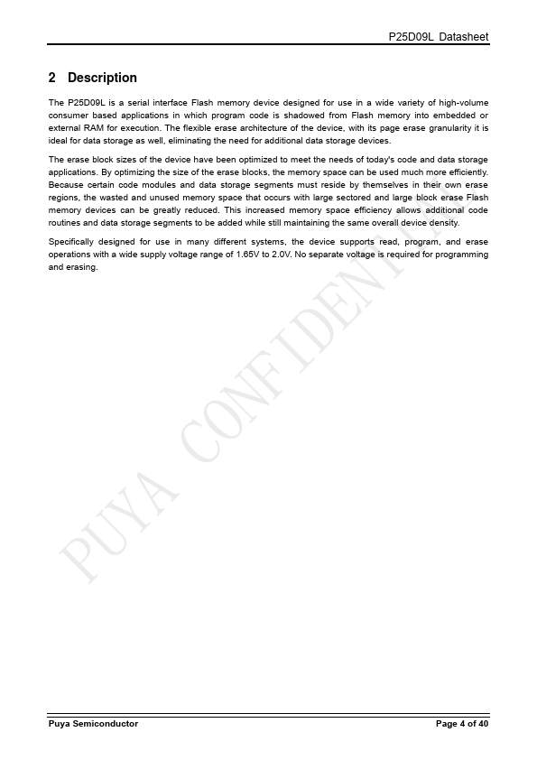
By optimizing the size of the erase blocks, the memory space can be used much more efficiently. Because certain code modules and data storage segments must reside by themselves in their own erase regions, the wasted and unused memory space that occurs with large sectored and large block erase Flash memory devices can be greatly reduced. This increased memory space efficiency allows additional code routines and data storage segments to be added while still maintaining the same overall device density. Specifically designed for use in many different systems, the device supports read, program, and erase operations with a wide supply voltage range of 1.65V to 2.0V. No separate voltage is required for programming and erasing. Puya Semiconductor Page 4 of 40 P25D09L Datasheet 3 Pin Definition 3.1 Pin Configurations CS# 1 8 SO 2 7 WP# 3 6 GND 4 5 VCC NC SLCK SI Vcc CS# 1 6 TOP View 2 5 CLK SI(IO0) SO(IO1) 3 4 GND 8-Lead SOP (150mil) and TSSOP 6-Pad USON(1.2x1.2mm) 3.2 Pin Descriptions No. Puya Semiconductor