FEATURES
Full CMOS, 6T Cell High Speed (Equal Access and Cycle Times) – 15/20/25/35 ns (Commercial/Industrial) – 20/25/35 ns (Military) Low Power Single TTL/CMOS Compatible Outputs Fully TTL Compatible Inputs Standard Pinout (JEDEC Approved) – 28-Pin 300 mil SOJ – 28-Pin 400 mil SOJ – 28-Pin 400 mil Ceramic DIP – 32-Pin Ceramic LCC 5V±10% Power Supply Data Retention with 2.0V Supply Three-State Outputs DESCRIPTION
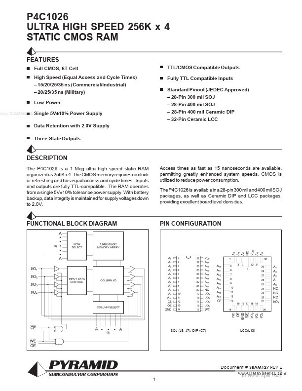
Inputs and outputs are fully TTL-compatible. With battery backup, data integrity is maintained for supply voltages down to 2.0V. Access times as fast as 15 nanoseconds are available, permitting greatly enhanced system speeds. CMOS is utilized to reduce power consumption. The P4C1026 is available in a 28-pin 300 mil and 400 mil SOJ packages, as well as Ceramic DIP and LCC packages, providing excellent board level densities. FUNCTIONAL BLOCK DIAGRAM PIN CONFIGURATION SOJ (J5, J7), DIP (C7) LCC(L13) Document # SRAM127 REV E 1 Revised April 2007 P4C1026 MAXIMUM RATINGS
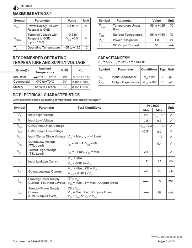
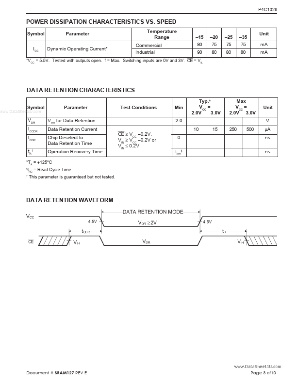
(1) Symbol... Pyramid Semiconductor