RF Micro Devices RF2416
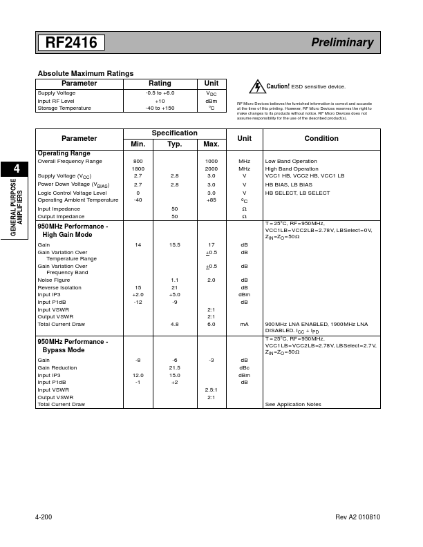
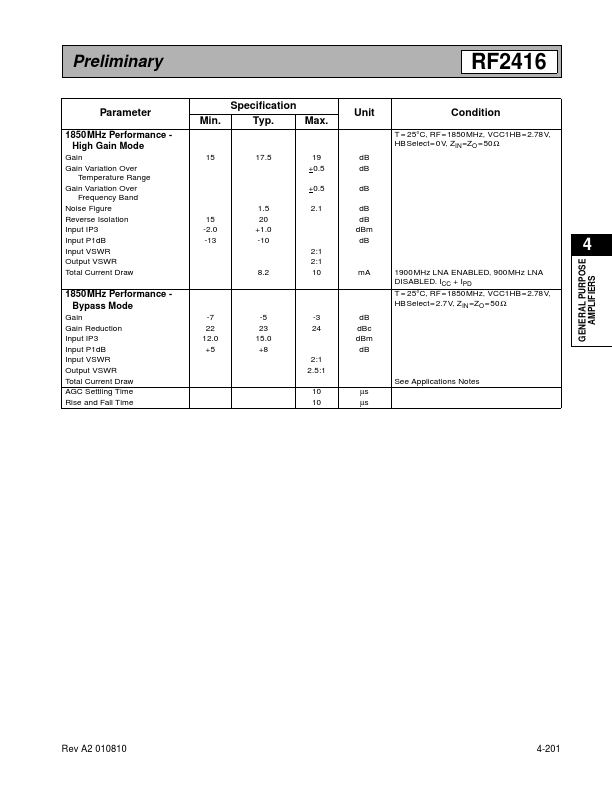
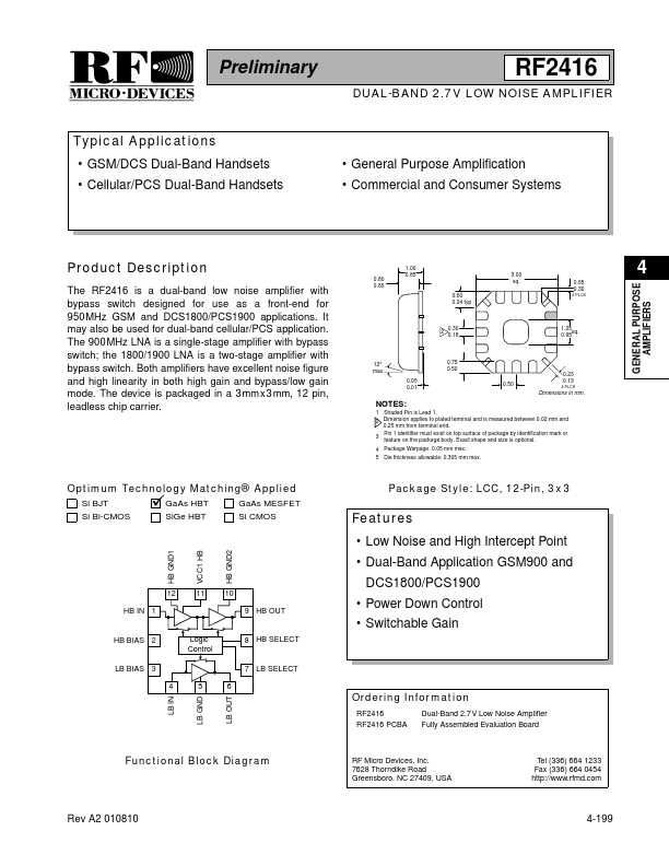
The RF2416 is a dual-band low noise amplifier with bypass switch designed for use as a front-end for 950MHz GSM and DCS1800/PCS1900 applications. It may also be used for dual-band cellular/PCS application. The 900MHz LNA is a single-stage amplifier with bypass switch; the 1800/1900 LNA is a two-stage amplifier with bypass switch.| Part No. | RF2416 |
|---|---|
| Datasheet | RF2416 Download |
| Manufacturer |  RF Micro Devices |
| Description | DUAL-BAND 2.7V LOW NOISE AMPLIFIER |
| Buy | Stock & Price |
APPLICATIONS
● GSM/DCS Dual-Band Handsets● Cellular/PCS Dual-Band Handsets RF2416 DUAL-BAND 2.7V LOW NOISE AMPLIFIER
● General Purpose Amplification
● Commercial and Consumer Systems Product
DESCRIPTION
Both amplifiers have excellent noise figure and high linearity in both high gain and bypass/low gain mode. The device is packaged in a 3mmx3mm, 12 pin, leadless chip carrier. 0.80 0.65 1.00 0.85 0.60 0.24 typ 4 PLCS 2 0.30 0.18 1.25 sq. 0.95 12° max 0.05 0.01 0.75 0.50 0.50 0.23 0.13 4 PLCS Dimensions in mm. NOTES: 1 Shaded Pin is Lead 1. 2 Dimension applies to plated terminal and is measured between 0.02 mm and 0.25 mm from terminal end. Pin 1 identifier must exist on top surface of package by identification mark or 3 feature on the package body. Exact shape and size is optional. 4 Package Warpage: 0.05 mm max. 5 Die thickness allowable: 0.305 mm max. Optimum Technology Matching® Applied Si BJT Si Bi-CMOS ü Package Style: LCC, 12-Pin, 3x3 GaAs HBT SiGe HBT GaAs MESFET Si CMOSFEATURES
...