1) Ultra small mold type. (VMN2) 2) Low high-frequency forward resistance / low
capacitance (CT). VMN2
zStructure
zConstruction Silicon epitaxial planar
zTaping dimensions (Unit : mm)
zAbsolute maximum ratings (Ta=25°C)
Parameter
Symbol
Reverse voltage Forward current Power dissipation
VR
IF Pd
Junction temperature
Tj
Storage temperature
Tstg
Limits 30 100 100 150
-55 to +150
Unit V mA
mW °C °C
zElectrical characteristics (Ta=25°C)
Parameter
Symbol Min. Typ. Max. Forward voltag.
The following content is an automatically extracted verbatim text
from the original manufacturer datasheet and is provided for reference purposes only.
View original datasheet text
PIN diode
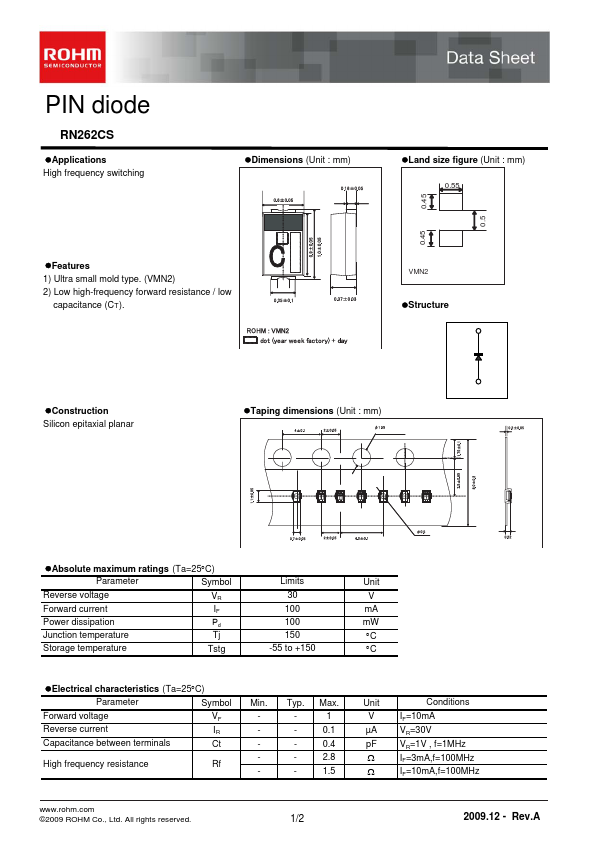
RN262CS
zApplications High frequency switching
zDimensions (Unit : mm)
zLand size figure (Unit : mm)
0.55
0.45 0.45 0.5
zFeatures 1) Ultra small mold type. (VMN2) 2) Low high-frequency forward resistance / low
capacitance (CT).
VMN2
zStructure
zConstruction Silicon epitaxial planar
zTaping dimensions (Unit : mm)
zAbsolute maximum ratings (Ta=25°C)
Parameter
Symbol
Reverse voltage Forward current Power dissipation
VR
IF Pd
Junction temperature
Tj
Storage temperature
Tstg
Limits 30 100 100 150
-55 to +150
Unit V mA
mW °C °C
zElectrical characteristics (Ta=25°C)
Parameter
Symbol Min. Typ. Max.
Forward voltage Reverse current Capacitance between terminals
VF - - 1 IR - - 0.1 Ct - - 0.4
High frequency resistance
Rf - - 2.8 - - 1.