VRS51L580
VRS51L580 is Versa 8051 MCUs manufactured by Ramtron.
- Part of the VRS51X570 comparator family.
- Part of the VRS51X570 comparator family.
Overview
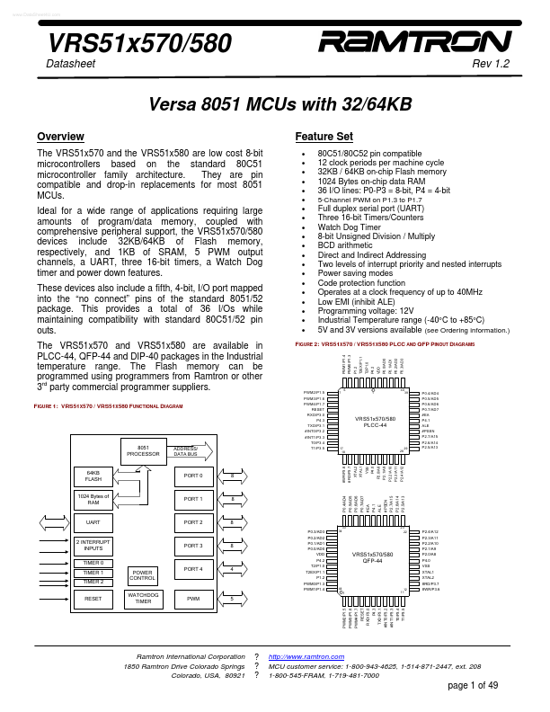
The VRS51x570 and the VRS51x580 are low cost 8-bit microcontrollers based on the standard 80C51 microcontroller family architecture. They are pin patible and drop-in replacements for most 8051 MCUs. Ideal for a wide range of applications requiring large amounts of program/data memory, coupled with prehensive peripheral support, the VRS51x570/580 devices include 32KB/64KB of Flash memory, respectively, and 1KB of SRAM, 5 PWM output channels, a UART, three 16-bit timers, a Watch Dog timer and power down features
. These devices also include a fifth, 4-bit, I/O port mapped into the “no connect” pins of the standard 8051/52 package. This provides a total of 36 I/Os while maintaining patibility with standard 80C51/52 pin outs. The VRS51x570 and VRS51x580 are available in PLCC-44, QFP-44 and DIP-40 packages in the Industrial temperature range. The Flash memory can be programmed using programmers from Ramtron or other 3rd party mercial programmer suppliers.
FIGURE 1: VRS51X570 / VRS51X580 FUNCTIONAL DIAGRAM
Feature
Set
- -
- -
- -
- -
- -
- -
- -
- -
- -
- -
80C51/80C52 pin patible 12 clock periods per machine cycle 32KB / 64KB on-chip Flash memory 1024 Bytes on-chip data RAM 36 I/O lines: P0-P3 = 8-bit, P4 = 4-bit
5-Channel PWM on P1.3 to P1.7
Full duplex serial port (UART) Three 16-bit Timers/Counters Watch Dog Timer 8-bit Unsigned Division / Multiply BCD arithmetic Direct and Indirect Addressing Two levels of interrupt priority and nested interrupts Power saving modes Code protection function Operates at a clock frequency of up to 40MHz Low EMI (inhibit ALE) Programming voltage: 12V Industrial Temperature range (-40°C to +85°C) 5V and 3V versions available (see Ordering information.)
FIGURE 2: VRS51X570 / VRS51X580 PLCC AND QFP PINOUT DIAGRAMS
PWM0/P1.3
PWM1/P1.4
P1.2 T2EX/P1.1
P0.0/AD0
P0.2/AD2
PWM2/P1.5 PWM3/P1.6 PWM4/P1.7 RESET RXD/P3.0 P4.3 TXD/P3.1 #INT0/P3.2 #INT1/P3.3 T0/P3.4 T1/P3.5
P0.3/AD3
40 39
P0.1/AD1
T2/P1.0
P4.2
P0.4/AD...