R8A66171SP
R8A66171SP is A2RT manufactured by Renesas.
- Part of the R8A66171DD comparator family.
- Part of the R8A66171DD comparator family.
DESCRIPTION
The R8A66171 is an integrated circuit for asynchronous serial data munications. It is used in bination with an 8-bit microprocessor and is produced using the silicon gate CMOS technology. R8A66171 is the succession product of M66230.
FEATURES
- Baud rate generator
- 4-byte FIFO data buffer for transmission and reception ..
- Error detection : CRC-CCITT
- Wakeup function
- Majority-voting system by sampling three points of received data
- Transmission / reception data format ( number of bits ) Start bit 1 Data bit 8 Wakeup bit 1 or nil Parity bit 1 or nil Stop bit 1 or 2
- Transmission speed 500Kbps (max)
- Access time ta (/RD-D) : 100ns
- High output current IOH=-24m A IOL=24m A Tx D, /RTS, P0, P1 pins
- Schmitt triggered input Rx D, /CTS, /RESET pins
- Wide operating supply voltage range (Vcc=3.0~3.6V or Vcc=4.5~5.5V)
- Wide operating temperature range (Ta=-40~85OC)
APPLICATION
Data munication control that uses microprocessor
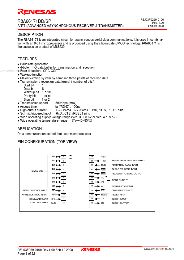
PIN CONFIGURATION (TOP VIEW)
D0 D1 D2 DATA BUS D3 D4 D5 D6 D7 READ CONTROL INPUT WRITE CONTROL INPUT RD WR
1 2 3 4 5 6 7 8 9 10 11 12
24 23 22 21 20 19 18 17 16 15 14 13
V CC Tx D Rx D CTS RTS P0 P1 INT CS RESET X1 X2 TRANSMISSION DATA OUTPUT RECEPTION DATA INPUT CLEAR-TO-SEND INPUT REQUEST-TO-SEND OUTPUT PORT OUTPUT INTERRUPT OUTPUT CHIP SELECT INPUT RESET INPUT CLOCK INPUT CLOCK OUTPUT
MAND/DATA C/D CONTROL INPUT GND
REJ03F269-0100 Rev.1.00 Feb.19.2008 Page 1 of 22
R8A66171DD/SP FUNCTION
The R8A66171 is a UART (Universal Asynchronous Receiver/Transmitter) and is used in the peripheral circuit of a MCU. The R8A66171 receives parallel data, converts into serial format, and then transmits the serial data via the Tx D pin. The device also receives data via the Rx D pin from external circuits and converts it into parallel format, and sends the parallel data via the data bus.
BLOCK DIAGRAM
Reset input mand/Data control input .. Read control input Write control input Chip select input
RESET C/D RD WR CS D0 D1 D2 D3
15 11 9 10...