RD74VT1G245 Description
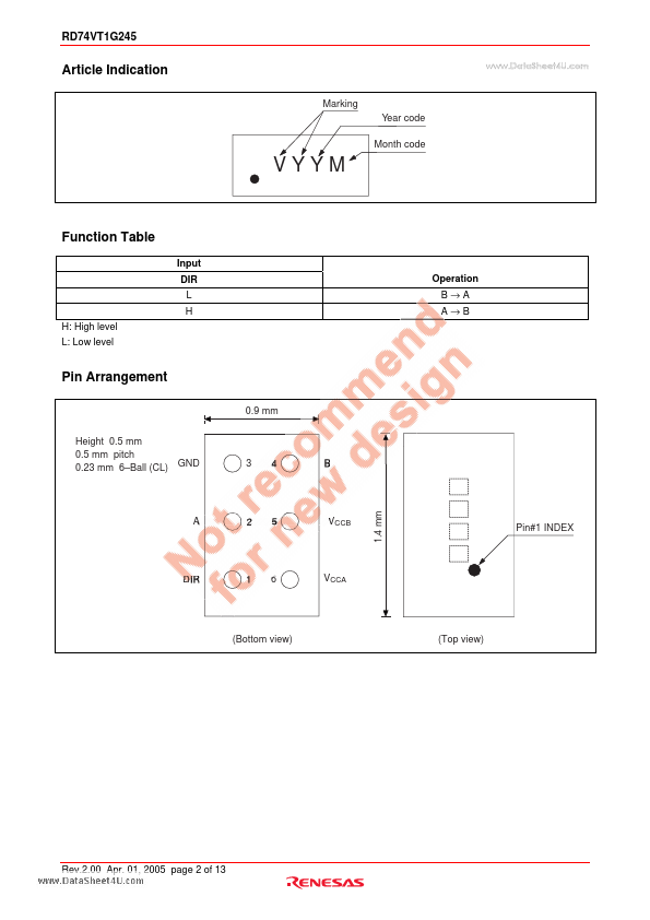
The RD74VT1G245 has one buffer in a 6 pin package. When DIR is high, data is transferred from the A inputs to the B outputs, and when DIR is low, data is transferred from the B inputs to the A outputs. And this product has two terminals (VCCA, VCCB), VCCA is connected with control input and A bus side VCCB is connected with B bus side.
RD74VT1G245 Key Features
- This product function as level shift transceiver that change VCCA input level to VCCB output level, VCCB input level to
- Supply voltage range: VCCA = 1.2 to 3.6 V VCCB = 1.2 to 3.6 V
- Operating temperature range: -40 to +85°C
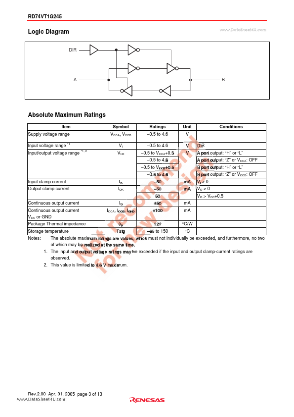
- Control input VI(max) = 3.6 V (@VCCA = 0 to 3.6 V)
- A bus side input outputs VI/O (max) = 3.6 V (@VCCA = 0 V or Output off state)
- B bus side input outputs VI/O (max) = 3.6 V (@VCCB = 0 V or Output off state)
- Ordering Information