RJK0389DPA
Features
- -
- -
- Low on-resistance Capable of 4.5 V gate drive High density mounting Pb-free Halogen-free
Outline
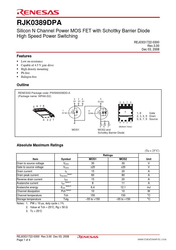
RENESAS Package code: PWSN0008DD-A (Package name: WPAK-D2)
2 3 4 D1 D1 D1
9 S1/D2
5 6 7 8
5 6 7 8
1 G1 8 G2
4 3 2 1
4 3 2 1
1, 8 Gate 2, 3, 4, 9 Drain 5, 6, 7, 9 Source
S2 S2 S2 5 6 7
(Bottom View)
MOS1
MOS2 and Schottky Barrier Diode
Absolute Maximum Ratings
(Ta = 25°C)
Ratings Item Drain to source voltage Gate to source voltage Drain current Drain peak current Reverse drain current Avalanche current Avalanche energy Channel dissipation Channel temperature Storage temperature Symbol VDSS VGSS ID ID(pulse)Note1 IDR IAP Note 2 EAR Note 2 Pch Note3 Tch Tstg MOS1 30 ±20 15 60 15 8 6.4 10 150
- 55 to +150 MOS2 30 ±20 20 80 20 11 12.1 10 150
- 55 to +150 Unit V V A A A A m J W °C
°C
Notes: 1. PW ≤ 10 µs, duty cycle ≤ 1% 2. Value at Tch = 25°C, Rg ≥ 50 Ω 3. Tc = 25°C
REJ03G1722-0300 Rev.3.00 Dec 03, 2008 Page 1 of 4
Electrical Characteristics
..
-...