RJK5015DPM
RJK5015DPM is Silicon N Channel MOS FET High Speed Power Switching manufactured by Renesas.
Features
- Low on-resistance
- Low leakage current
- High speed switching REJ03G1753-0100 Rev.1.00 Oct 26, 2009
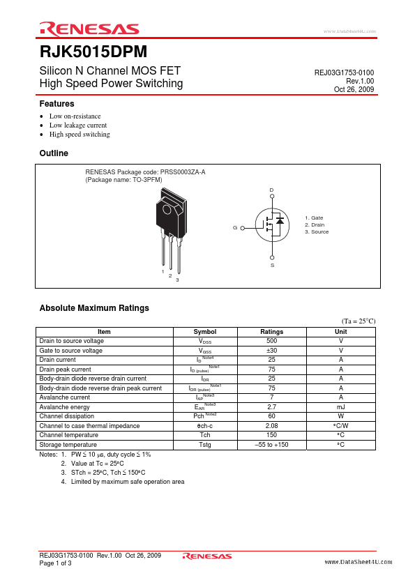
Outline
RENESAS Package code: PRSS0003ZA-A (Package name: TO-3PFM)
1. Gate 2. Drain 3. Source
S 1 2 3
Absolute Maximum Ratings
(Ta = 25°C)
Item Drain to source voltage Gate to source voltage Drain current Drain peak current Body-drain diode reverse drain current Body-drain diode reverse drain peak current Avalanche current Avalanche energy Channel dissipation Channel to case thermal impedance Channel temperature Storage temperature Notes: 1. 2. 3. 4. PW ≤ 10 μs, duty cycle ≤ 1% Value at Tc = 25°C STch = 25°C, Tch ≤ 150°C Limited by maximum safe operation area Symbol VDSS VGSS Note4 ID ID (pulse) IDR Note1 IDR (pulse) Note3 IAP EARNote3 Pch Note2 θch-c Tch Tstg
Note1
Ratings 500 ±30 25 75 25 75 7 2.7 60 2.08 150
- 55 to +150
Unit V V A A A A A m J W °C/W °C °C
REJ03G1753-0100 Rev.1.00 Oct 26, 2009 Page 1 of 3
..
Electrical Characteristics
(Ta = 25°C)
Item Drain to source breakdown voltage Zero gate voltage drain current Gate to source leak current Gate to source cutoff voltage Static drain to source on state resistance Input capacitance Output capacitance Reverse transfer capacitance Turn-on delay time Rise time Turn-off delay time Fall time Total gate charge Gate to source charge Gate to drain charge Body-drain diode forward voltage Body-drain diode reverse recovery time Notes: 5. Pulse test Symbol V(BR)DSS IDSS IGSS VGS(off) RDS(on) Ciss Coss Crss td(on) tr td(off) tf Qg Qgs Qgd VDF trr Min 500
- - 3.0
- -
- -
- -
- -
- -
- -
- Typ
- -
- - 0.21 2600 270 32 42 59 103 45 66 14 29 0.96 380 Max
- 1 ±0.1 4.5 0.24
- -
- -
- -
- -
- - 1.60
- Unit V μA μA V Ω p F p F p F ns ns ns ns n C n C n C V ns Test conditions ID = 10 m A, VGS = 0 VDS = 500 V, VGS = 0 VGS = ±30 V, VDS = 0 VDS = 10 V, ID = 1 m A ID = 12.5 A, VGS = 10 V Note5 VDS = 25 V VGS = 0 f = 1 MHz ID = 12.5 A VGS = 10 V RL = 20 Ω Rg = 10 Ω VDD = 400 V VGS = 10 V ID = 25 A IF = 25 A, VGS...