2305
2305 is 3.3V Zero-Delay Clock Buffer manufactured by Renesas.
Description
The 2305 is a high-speed phase-lock loop (PLL) clock buffer, designed to address high-speed clock distribution applications. The zero-delay is achieved by aligning the phase between the ining clock and the output clock, operable within the range of 10MHz to 133MHz.
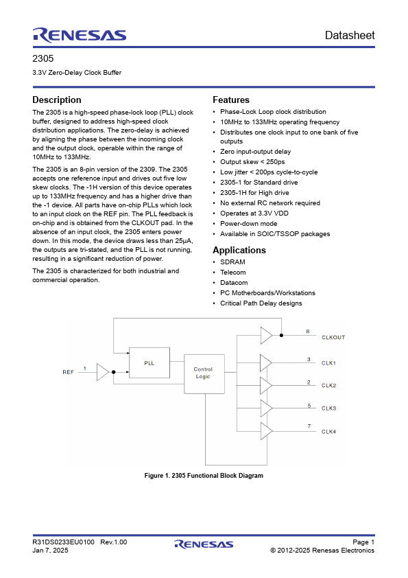
The 2305 is an 8-pin version of the 2309. The 2305 accepts one reference input and drives out five low skew clocks. The -1H version of this device operates up to 133MHz frequency and has a higher drive than the -1 device. All parts have on-chip PLLs which lock to an input clock on the REF pin. The PLL feedback is on-chip and is obtained from the CLKOUT pad. In the absence of an input clock, the 2305 enters power down. In this mode, the device draws less than 25µA, the outputs are tri-stated, and the PLL is not running, resulting in a significant reduction of power.
The 2305 is characterized for both industrial and mercial operation.
Features
- Phase-Lock Loop clock distribution
- 10MHz to 133MHz operating frequency
- Distributes one clock input to one bank of five outputs
- Zero input-output delay
- Output skew < 250ps
- Low jitter < 200ps cycle-to-cycle
- 2305-1 for Standard drive
- 2305-1H for High drive
- No external RC network required
- Operates at 3.3V VDD
- Power-down mode
- Available in SOIC/TSSOP packages
Applications
- SDRAM
- Tele
- Data
- PC Motherboards/Workstations
- Critical Path Delay designs
Figure 1. 2305 Functional Block Diagram
R31DS0233EU0100 Rev.1.00 Jan 7, 2025
Page 1 © 2012-2025 Renesas Electronics
2305 Datasheet
Contents
1. Pin Information
- -
- -
- -
- -
- -
- -
- -
- - 3 1.1 Pin Assignments
- -
- -
-...