551S
Description
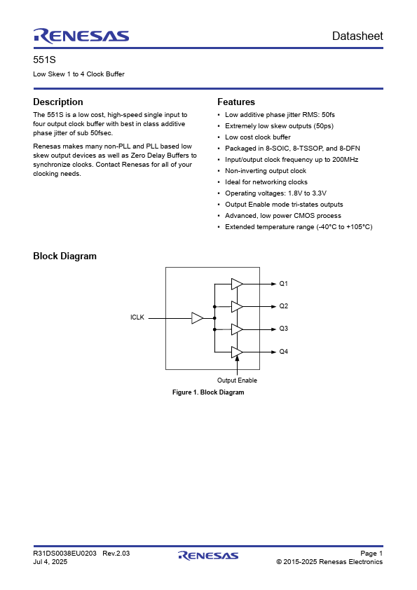
The 551S is a low cost, high-speed single input to four output clock buffer with best in class additive phase jitter of sub 50fsec. Renesas makes many non-PLL and PLL based low skew output devices as well as Zero Delay Buffers to synchronize clocks.