74FCT38072S Overview
Key Specifications
Package: SOIC
Mount Type: Surface Mount
Pins: 8
Operating Voltage: 1.8 V
Description
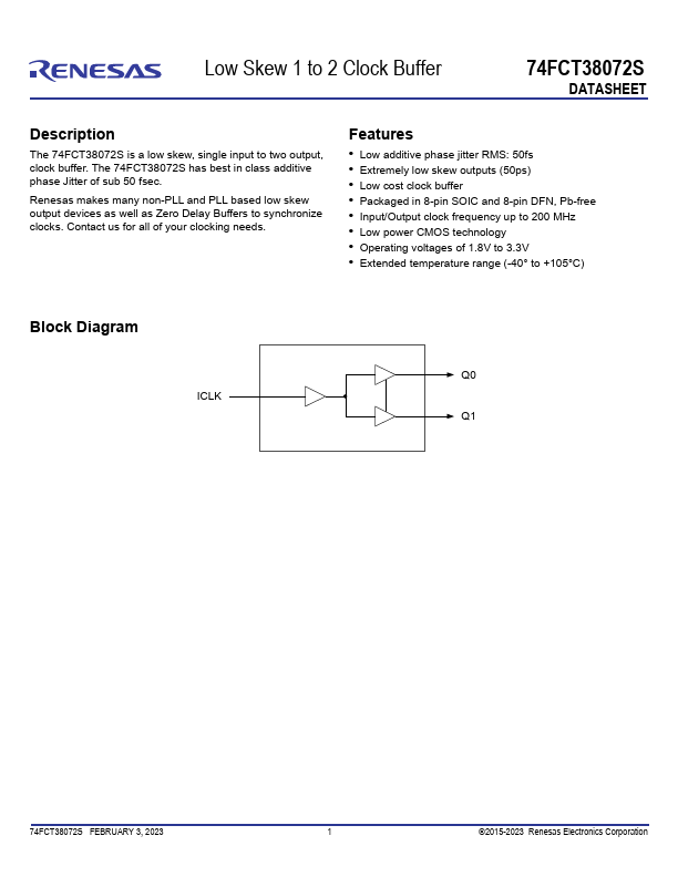
The 74FCT38072S is a low skew, single input to two output, clock buffer. The 74FCT38072S has best in class additive phase Jitter of sub 50 fsec.
Key Features
- Low additive phase jitter RMS: 50fs
- Extremely low skew outputs (50ps)
- Low cost clock buffer
- Packaged in 8-pin SOIC and 8-pin DFN, Pb-free
- Input/Output clock frequency up to 200 MHz