854S01I
Description
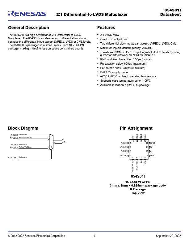
The 854S01I is a high performance 2:1 Differential-to-LVDS Multiplexer. The 854S01I can also perform differential translation because the differential inputs accept LVPECL, LVDS or CML levels. The 854S01I is packaged in a small 3mm x 3mm 16 VFQFPN package, making it ideal for use on space constrained boards.
Features
- 2:1 LVDS MUX
- One LVDS output pair
- Two differential clock inputs can accept: LVPECL, LVDS, CML
- Maximum input/output frequency: 2.5GHz
- Translates LVCMOS/LVTTL input signals to LVDS levels by using a resistor bias network on n PCLK0, n PCLK1
- RMS additive phase jitter: 0.06ps (typical)
- Propagation delay: 600ps (maximum)
- Part-to-part skew: 350ps (maximum)
- Full 3.3V supply mode
- -40°C to 85°C ambient operating temperature
- Supports case temperature up to +105°C
- Available in lead-free (Ro HS 6) package
Block Diagram
PCLK0 Pulldown n PCLK0 Pullup/Pulldown
PCLK1 Pulldown n PCLK1 Pullup/Pulldown
CLK_SEL Pulldown
0 Q n Q
Pin Assignment nc GND GND...