87974I
87974I is LVCMOS/LVTTL Clock Generator manufactured by Renesas.
Low Skew, 1-to-15, LVCMOS/LVTTL Clock Generator
Data Sheet
GENERAL DESCRIPTION
The 87974I is a low skew, low jitter 1-to-15 LVCMOS/ LVTTL Clock Generator/Zero Delay Buffer. The device has a fully integrated PLL and three banks whose divider ratios can be independently controlled, providing output frequency relationships of 1:1, 2:1, 3:1, 3:2, 3:2:1. In addition, the external feedback connection provides for a wide selection of output-to-input frequency ratios. The CLK0 and CLK1 pins allow for redundant clocking on the input and dynamically switching the PLL between two clock sources.
Guaranteed low jitter and output skew characteristics make the 87974I ideal for those applications demanding well defined performance and repeatability.
Features
- Fully integrated PLL
- Fifteen single ended 3.3V LVCMOS/LVTTL outputs
- Two LVCMOS/LVTTL clock inputs for redundant clock applica- tions
- CLK0 and CLK1 accepts the following input levels:
LVCMOS/LVTTL
- Output frequency range: 8.33MHz to 125MHz
- VCO range: 200MHz to 500MHz
- External feedback for ”zero delay” clock regeneration
- Cycle-to-cycle jitter: ±100ps (typical)
- Output skew: 350ps (maximum)
- 3.3V operating supply
- -40°C to 85°C ambient operating temperature
- Available in lead-free Ro HS-pliant package
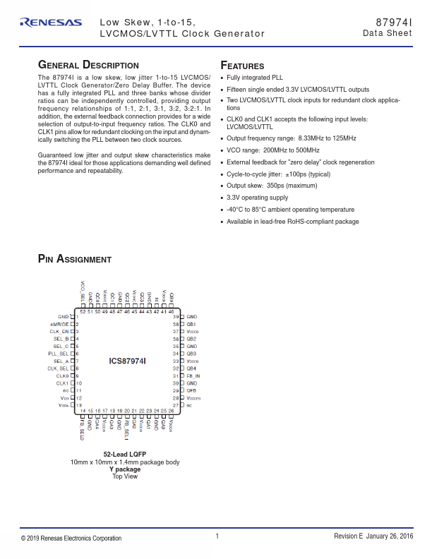
PIN ASSIGNMENT
52-Lead LQFP
10mm x 10mm x 1.4mm package body Y package Top View
©2016 Integrated Device Technology, Inc
Revision E January 26, 2016
BLOCK DIAGRAM
87974I Data Sheet
©2016 Integrated Device Technology, Inc
Revision E January 26, 2016
87974I Data Sheet
SIMPLIFIED BLOCK...