8SLVD2102
8SLVD2102 is Dual 1:2 LVDS Output Fanout Buffer manufactured by Renesas.
Description
The 8SLVD2102 is a high-performance differential dual 1:2 LVDS fanout buffer. The device is designed for the fanout of high-frequency, very low additive phase-noise clock and data signals. The 8SLVD2102 is characterized to operate from a 2.5V power supply. Guaranteed output-to-output and part-to-part skew characteristics make the 8SLVD2102 ideal for those clock distribution applications demanding well-defined performance and repeatability.
Two independent buffers with two low skew outputs each are available. The integrated bias voltage generators enables easy interfacing of single-ended signals to the device inputs. The device is optimized for low power consumption and low additive phase noise.
Features
- Two 1:2, low skew, low additive jitter LVDS fanout buffers
- Two differential clock inputs
- Differential pairs can accept the following differential input levels: LVDS and LVPECL
- Maximum input clock frequency: 2GHz
- Output bank skew: 15ps (maximum)
- Propagation delay: 300ps (maximum)
- Low additive phase jitter: 200fs, RMS (maximum); f REF = 156.25MHz, VPP = 1V, VCMR = 1V, Integration Range 10k Hz
- 20MHz
- 2.5V supply voltage
- Maximum device current consumption (IDD): 90m A
- Lead-free (Ro HS 6) 16-Lead VFQFPN package
- -40°C to 85°C ambient operating temperature
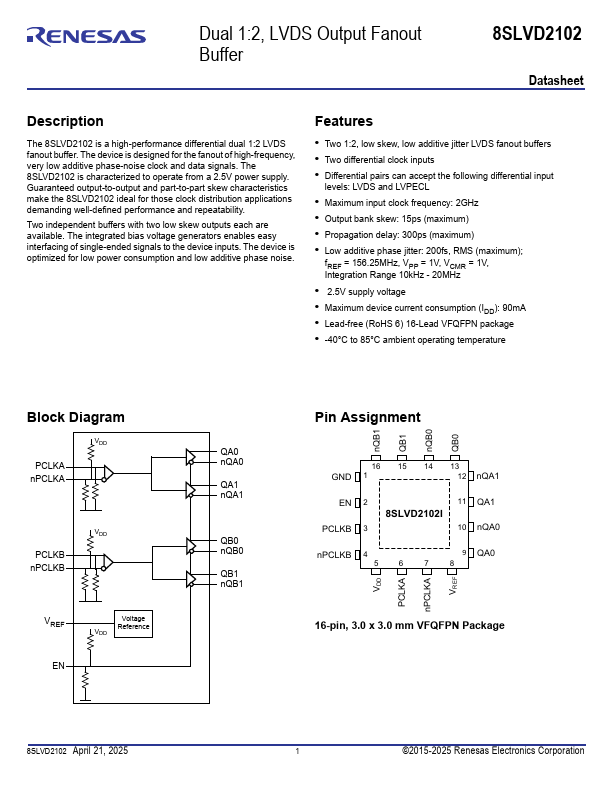
Block Diagram
PCLKA n PCLKA
PCLKB n PCLKB
VREF EN
Voltage VDD Reference
QA0 n QA0
QA1 n QA1
QB0 n QB0
QB1 n QB1
Pin Assignment n QB1 QB1 n QB0 QB0
16 15 14 13
GND 1
12 n QA1
EN 2 PCLKB 3
8SLVD2102I
8XXXXXX
11 QA1 10 n QA0 n PCLKB 4
9...