8SLVP1204
8SLVP1204 is LVPECL Output Fanout Buffer manufactured by Renesas.
Description
The 8SLVP1204 is a high-performance differential LVPECL fanout buffer. The device is designed for the fanout of high-frequency, very low additive phase-noise clock and data signals. The 8SLVP1204 is characterized to operate from a 3.3V or 2.5V power supply.
Guaranteed output-to-output and part-to-part skew characteristics make the 8SLVP1204 ideal for clock distribution applications that demand well-defined performance and repeatability. Two selectable differential inputs and four low skew outputs are available. The integrated bias voltage reference enables easy interfacing of single-ended signals to the device inputs. The device is optimized for low power consumption and low additive phase noise.
Features
- Four low skew, low additive jitter LVPECL output pairs
- Two selectable, differential clock input pairs
- Differential PCLKx pairs can accept the following differential input levels: LVDS, LVPECL, CML
- Differential PCLKx pairs can also accept single-ended LVCMOS levels. See Applications Information, “Wiring the Differential Input to Accept Single-Ended Levels” (Figures 1A and 1B)
- Maximum input clock frequency: 2GHz
- LVCMOS interface levels for the control input, (input select)
- Output skew: 5ps (typical), at 3.63V
- Propagation delay: 200ps (typical), at 3.63V
- Low additive phase jitter, RMS; f REF = 156.25MHz, VPP = 1V,
12k Hz
- 20MHz: 40fs (maximum), at 3.63V
- Maximum device current consumption (IEE): 60m A (maximum), at 3.63V
- Full 3.3V±5%, 3.3V±10% or 2.5V±5% supply
- Lead-free (Ro HS 6), 16-Lead VFQFPN packaging
- -40°C to 85°C ambient operating temperature
- Supports case temperature 105°C operations
- Supports PCI Express Gen1- 5
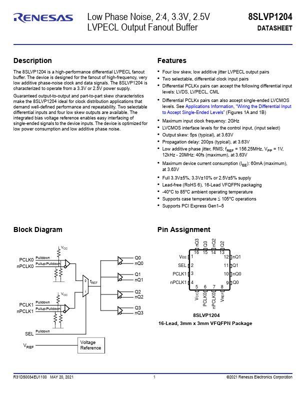
Block Diagram
PCLK0 Pulldown n PCLK0 Pullup/Pulldown
PCLK1 Pulldown n PCLK1 Pullup/Pulldown
0 f REF 1
SEL Pulldown VREF
Voltage Reference
Pin Assignment n Q3 Q3 n Q2 Q2
16 15 14 13
Q0
VEE 1
12 n Q1 n Q0
SEL 2
11 Q1
Q1
PCLK1 3
10 n Q0 n Q1 n PCLK1 4
9...