8T74S208B
Description
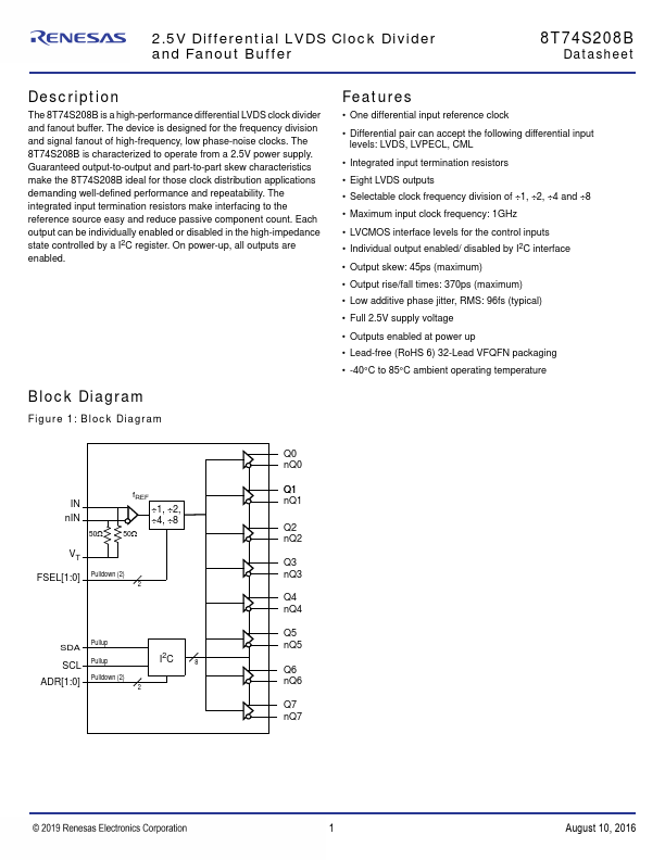
The 8T74S208B is a high-performance differential LVDS clock divider and fanout buffer.
Key Features
- One differential input reference clock
- Differential pair can accept the following differential input levels: LVDS, LVPECL, CML
- Integrated input termination resistors
- Eight LVDS outputs
- Maximum input clock frequency: 1GHz
- LVCMOS interface levels for the control inputs
- Individual output enabled/ disabled by I2C interface
- Output skew: 45ps (maximum)
- Output rise/fall times: 370ps (maximum)
- Low additive phase jitter, RMS: 96fs (typical)