9DBV0631 Overview
Key Specifications
Mount Type: Surface Mount
Pins: 40
Operating Voltage: 1.8 V
Max Voltage (typical range): 1.9 V
Description
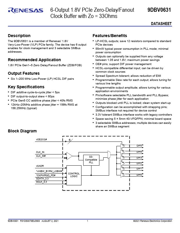
The 9DBV0631 is a member of Renesas’ 1.8V Very-Low-Power (VLP) PCIe family. The device has 6 output enables for clock management and 3 selectable SMBus addresses.
Key Features
- Six 1–200 MHz Low-Power (LP) HCSL DIF pairs Key Specifications
- DIF additive cycle-to-cycle jitter < 5ps
- DIF output-to-output skew < 60ps
- PCIe Gen5 CC additive phase jitter < 40fs RMS
- 12kHz–20MHz additive phase jitter = 156fs RMS at 156.25MHz (typical)