9DML4493A Overview
Key Specifications
Mount Type: Surface Mount
Pins: 32
Operating Voltage: 1.8 V
Max Voltage (typical range): 1.89 V
Description
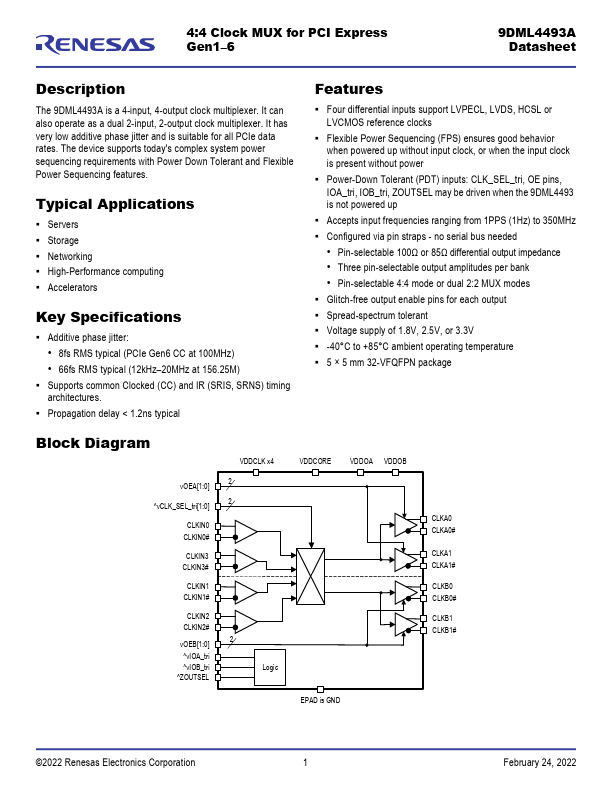
The 9DML4493A is a 4-input, 4-output clock multiplexer. It can also operate as a dual 2-input, 2-output clock multiplexer.
Key Features
- no serial bus needed
- Pin-selectable 100Ω or 85Ω differential output impedance
- Three pin-selectable output amplitudes per bank