9FGL0241
Overview
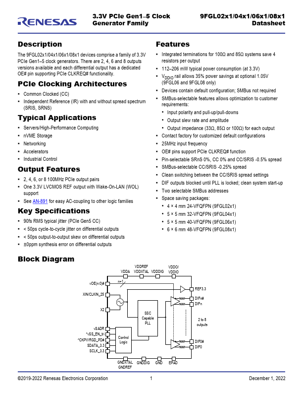
The 9FGL02x1/04x1/06x1/08x1 devices comprise a family of 3.3V PCIe Gen1-5 clock generators. There are 2, 4, 6 and 8 outputs versions available and each differential output has a dedicated OE# pin supporting PCIe CLKREQ# functionality.
- Input polarity and pull-up/pull-downs
- Output slew rate and amplitude
- Output impedance (33Ω, 85Ω or 100Ω) for each output; Contact factory for customized default configurations; 25MHz input frequency; OE# pins support PCIe CLKREQ# function; Pin-selectable SRnS 0%, CC 0% and CC/SRIS -0.5% spread; SMBus-selectable CC/SRIS -0.25% spread; Clean switching between the CC/SRIS spread settings; DIF outputs blocked until PLL is locked; clean system start-up; Two selectable SMBus addresses; Space saving packages:
- 4 × 4 mm 24-VFQFPN (9FGL02x1)
- 5 × 5 mm 32-VFQFPN (9FGL04x1)
- 5 × 5 mm 40-