Datasheet4U Logo Datasheet4U.com

9FGL0251D - 3.3V PCIe Gen1-6 Clock Generator

Download the 9FGL0251D datasheet PDF. This datasheet also covers the 9FGL0241D variant, as both devices belong to the same 3.3v pcie gen1-6 clock generator family and are provided as variant models within a single manufacturer datasheet.

General Description

2.

.

Key Features

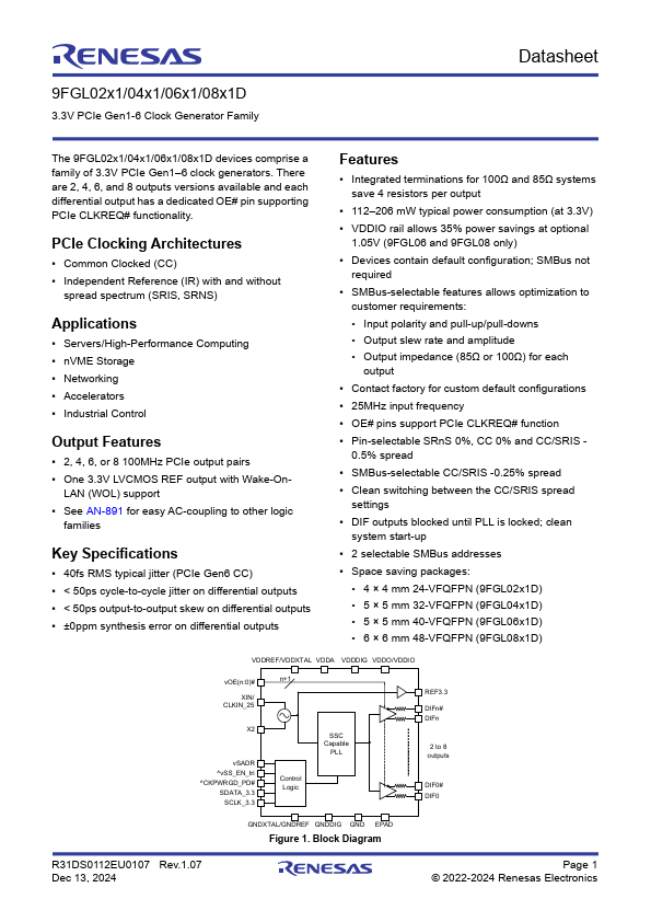
  • 2, 4, 6, or 8 100MHz PCIe output pairs.
  • One 3.3V LVCMOS REF output with Wake-On- LAN (WOL) support.
  • See AN-891 for easy AC-coupling to other logic families Key Specifications.
  • 40fs RMS typical jitter (PCIe Gen6 CC).
  • < 50ps cycle-to-cycle jitter on differential outputs.
  • < 50ps output-to-output skew on differential outputs.
  • ±0ppm synthesis error on differential outputs Features.
  • Integrated terminations for 100Ω and 85Ω systems save 4 resistors per output.

📥 Download Datasheet

Note: The manufacturer provides a single datasheet file (9FGL0241D-Renesas.pdf) that lists specifications for multiple related part numbers.

Datasheet Details

Part number 9FGL0251D
Manufacturer Renesas
File Size 1.39 MB
Description 3.3V PCIe Gen1-6 Clock Generator
Datasheet download datasheet 9FGL0251D Datasheet

Full PDF Text Transcription (Reference)

The following content is an automatically extracted verbatim text from the original manufacturer datasheet and is provided for reference purposes only.

View original datasheet text
9FGL02x1/04x1/06x1/08x1D 3.3V PCIe Gen1-6 Clock Generator Family Datasheet The 9FGL02x1/04x1/06x1/08x1D devices comprise a family of 3.3V PCIe Gen1–6 clock generators. There are 2, 4, 6, and 8 outputs versions available and each differential output has a dedicated OE# pin supporting PCIe CLKREQ# functionality. PCIe Clocking Architectures ▪ Common Clocked (CC) ▪ Independent Reference (IR) with and without spread spectrum (SRIS, SRNS) Applications ▪ Servers/High-Performance Computing ▪ nVME Storage ▪ Networking ▪ Accelerators ▪ Industrial Control Output Features ▪ 2, 4, 6, or 8 100MHz PCIe output pairs ▪ One 3.