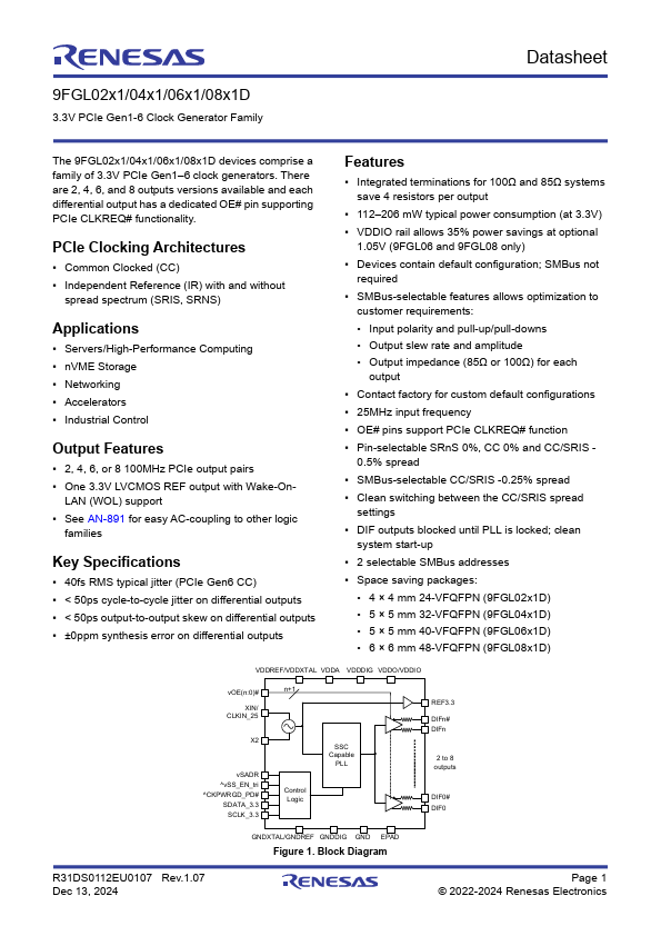
| Part | 9FGL0451D |
|---|---|
| Description | 3.3V PCIe Gen1-6 Clock Generator |
| Manufacturer | Renesas |
| Size | 1.39 MB |
Pricing from 3.05246 USD, available from DigiKey and Avnet.
Price & Availability
| Seller | Inventory | Price Breaks | Buy |
|---|---|---|---|
| DigiKey | 0 | 2500+ : 3.05246 USD | View Offer |
| Avnet | 0 | 2500+ : 3 USD 5000+ : 2.83784 USD 10000+ : 2.78871 USD 20000+ : 2.77448 USD |
View Offer |
Related Datasheets
| Part Number | Manufacturer | Description |
|---|---|---|
| 9FGL0451 | IDT | 4-Output 3.3V PCIe Clock Generator |

