9FGL0841
9FGL0841 is 3.3V PCIe Gen1-5 Clock Generator manufactured by Renesas.
- Part of the 9FGL0241 comparator family.
- Part of the 9FGL0241 comparator family.
Description
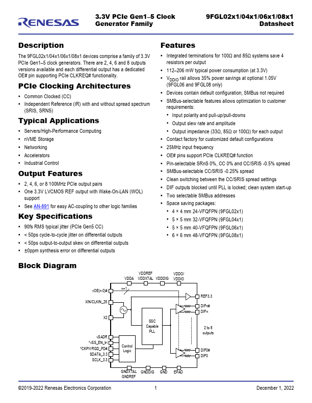
The 9FGL02x1/04x1/06x1/08x1 devices prise a family of 3.3V PCIe Gen1- 5 clock generators. There are 2, 4, 6 and 8 outputs versions available and each differential output has a dedicated OE# pin supporting PCIe CLKREQ# functionality.
PCIe Clocking Architectures
- mon Clocked (CC)
- Independent Reference (IR) with and without spread spectrum
(SRIS, SRNS)
Typical Applications
- Servers/High-Performance puting
- n VME Storage
- Networking
- Accelerators
- Industrial Control
Output Features
- 2, 4, 6, or 8 100MHz PCIe output pairs
- One 3.3V LVCMOS REF output with Wake-On-LAN (WOL) support
- See AN-891 for easy AC-coupling to other logic families
Key Specifications
- 90fs RMS typical jitter (PCIe Gen5 CC)
- < 50ps cycle-to-cycle jitter on differential outputs
- < 50ps output-to-output skew on differential outputs
- ±0ppm synthesis error on differential outputs
Features
- Integrated terminations for 100Ω and 85Ω systems save 4 resistors per output
- 112- 206 m W typical power consumption (at 3.3V)
- VDDIO rail allows 35% power savings at optional 1.05V
(9FGL06 and 9FGL08 only)
- Devices contain default configuration; SMBus not required
- SMBus-selectable features allows optimization to customer requirements:
- Input polarity and pull-up/pull-downs
- Output slew rate and amplitude
- Output impedance (33Ω, 85Ω or 100Ω) for each output
- Contact factory for customized default configurations
- 25MHz input frequency
- OE# pins support PCIe CLKREQ# function
- Pin-selectable SRn S 0%, CC 0% and CC/SRIS -0.5% spread
- SMBus-selectable CC/SRIS -0.25% spread
- Clean switching between the CC/SRIS spread settings
- DIF outputs blocked until PLL is locked; clean system start-up
- Two selectable SMBus addresses
- Space saving...