9FGL0841D
9FGL0841D is 3.3V PCIe Gen1-6 Clock Generator manufactured by Renesas.
- Part of the 9FGL0241D comparator family.
- Part of the 9FGL0241D comparator family.
Features
- 2, 4, 6, or 8 100MHz PCIe output pairs
- One 3.3V LVCMOS REF output with Wake-On-
LAN (WOL) support
- See AN-891 for easy AC-coupling to other logic families
Key Specifications
- 40fs RMS typical jitter (PCIe Gen6 CC)
- < 50ps cycle-to-cycle jitter on differential outputs
- < 50ps output-to-output skew on differential outputs
- ±0ppm synthesis error on differential outputs
Features
- Integrated terminations for 100Ω and 85Ω systems save 4 resistors per output
- 112- 206 m W typical power consumption (at 3.3V)
- VDDIO rail allows 35% power savings at optional
1.05V (9FGL06 and 9FGL08 only)
- Devices contain default configuration; SMBus not required
- SMBus-selectable features allows optimization to customer requirements:
- Input polarity and pull-up/pull-downs
- Output slew rate and amplitude
- Output impedance (85Ω or 100Ω) for each output
- Contact factory for custom default configurations
- 25MHz input frequency
- OE# pins support PCIe CLKREQ# function
- Pin-selectable SRn S 0%, CC 0% and CC/SRIS
- 0.5% spread
- SMBus-selectable CC/SRIS -0.25% spread
- Clean switching between the CC/SRIS spread settings
- DIF outputs blocked until PLL is locked; clean system start-up
- 2 selectable SMBus addresses
- Space saving packages:
- 4 × 4 mm 24-VFQFPN (9FGL02x1D)
- 5 × 5 mm 32-VFQFPN (9FGL04x1D)
- 5 × 5 mm 40-VFQFPN (9FGL06x1D)
- 6 × 6 mm 48-VFQFPN (9FGL08x1D)
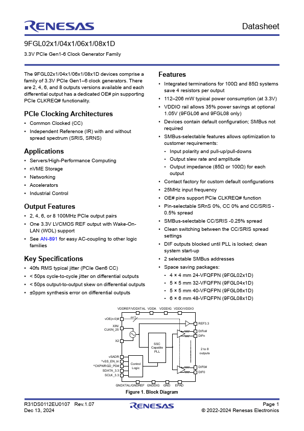
VDDREF/VDDXTAL VDDA VDDDIG VDDO/VDDIO v OE(n:0)# XIN/
CLKIN_25
X2 v SADR ^v SS_EN_tri ^CKPWRGD_PD# SDATA_3.3
SCLK_3.3 n+1
Control Logic
SSC...