9FGV0841 Overview
Key Specifications
Package: 100
Mount Type: Surface Mount
Pins: 48
Operating Voltage: 1.8 V
Description
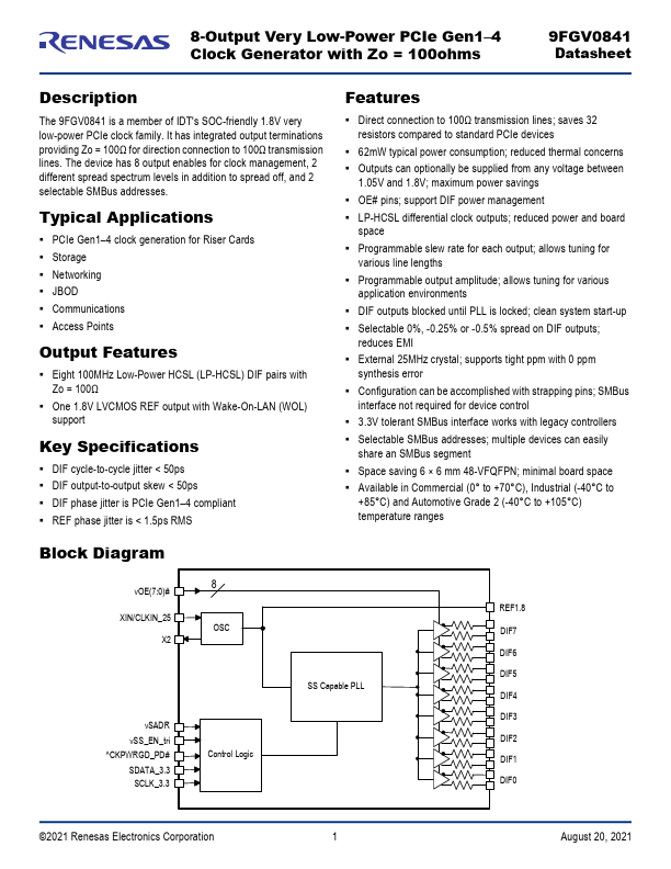
The 9FGV0841 is a member of IDT's SOC-friendly 1.8V very low-power PCIe clock family. It has integrated output terminations providing Zo = 100Ω for direction connection to 100Ω transmission lines.