Datasheet4U Logo Datasheet4U.com

9FGV1002C - PCIe Gen1-5 Low-Power PhiClock Generators

Datasheet Summary

Description

The 9FGV1002C / 9FGV1006C are members of the Renesas’ PhiClock™ programmable clock generator family.

These devices are optimized for low phase noise spread-spectrum applications such as PCIe® Express.

Features

  • 2 or 4 programmable output pairs plus 1 or 2 LVCMOS REF outputs.
  • 1MHz.
  • 325MHz LVDS or LP-HCSL outputs.
  • 1MHz.
  • 200MHz LVCMOS outputs Features.
  • 1.8V, 2.5V or 3.3V core power supplies.
  • Individual 1.8V, 2.5V or 3.3V VDDO for each output pair.
  • -40°C to +85°C operation.
  • standard product.
  • -40°C to +105°C operation.
  • 9FGV1002C automotive product.
  • Direct connection to HCSL, LVDS and LVCMOS inputs.
  • Renesas’ LP-HCSL technology imp.

📥 Download Datasheet

Datasheet preview – 9FGV1002C

Datasheet Details

Part number 9FGV1002C
Manufacturer Renesas
File Size 1.11 MB
Description PCIe Gen1-5 Low-Power PhiClock Generators
Datasheet download datasheet 9FGV1002C Datasheet
Additional preview pages of the 9FGV1002C datasheet.
Other Datasheets by Renesas

Full PDF Text Transcription

Click to expand full text
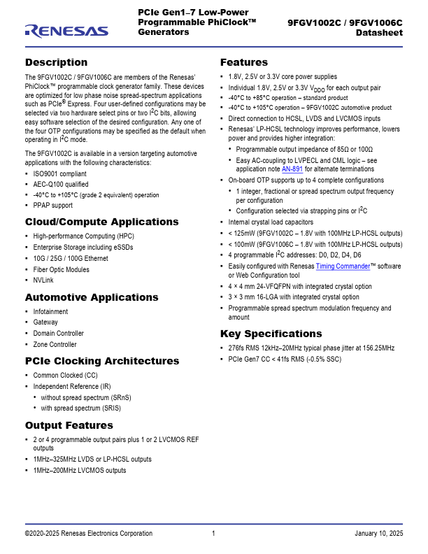
PCIe Gen1–7 Low-Power Programmable PhiClock™ Generators 9FGV1002C / 9FGV1006C Datasheet Description The 9FGV1002C / 9FGV1006C are members of the Renesas’ PhiClock™ programmable clock generator family. These devices are optimized for low phase noise spread-spectrum applications such as PCIe® Express. Four user-defined configurations may be selected via two hardware select pins or two I2C bits, allowing easy software selection of the desired configuration. Any one of the four OTP configurations may be specified as the default when operating in I2C mode.
Published: |