9SQL4952C Overview
Key Specifications
Operating Voltage: 3.3 V
Max Voltage (typical range): 3.465 V
Min Voltage (typical range): 3.135 V
Length: 4 mm
Description
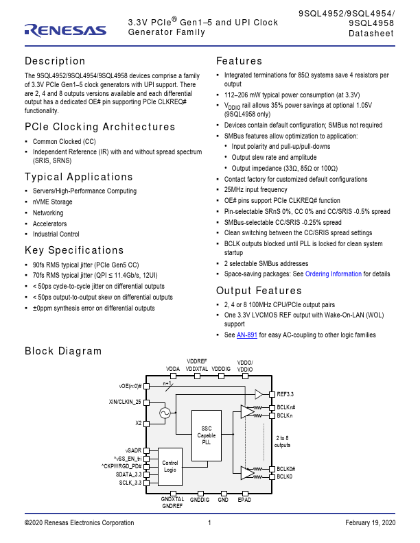
The 9SQL4952/9SQL4954/9SQL4958 devices comprise a family of 3.3V PCIe Gen1–5 clock generators with UPI support. There are 2, 4 and 8 outputs versions available and each differential output has a dedicated OE# pin supporting PCIe CLKREQ# functionality.
Key Features
- Input polarity and pull-up/pull-downs
- Output slew rate and amplitude