9SQL4954C Datasheet Text
3.3V PCIe® Gen1- 5 and UPI Clock Generator Family
9SQL4952/9SQL4954/ 9SQL4958 Datasheet
Description
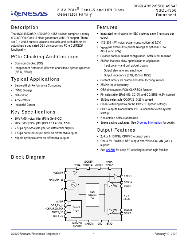
The 9SQL4952/9SQL4954/9SQL4958 devices prise a family of 3.3V PCIe Gen1- 5 clock generators with UPI support. There are 2, 4 and 8 outputs versions available and each differential output has a dedicated OE# pin supporting PCIe CLKREQ# functionality.
PCIe Clocking Architectures
- mon Clocked (CC)
- Independent Reference (IR) with and without spread spectrum
(SRIS, SRNS)
Typical Applications
- Servers/High-Performance puting
- nVME Storage
- Networking
- Accelerators
- Industrial Control
Key Specifications
- 90fs RMS typical jitter (PCIe Gen5 CC)
- 70fs RMS typical jitter (QPI ≤ 11.4Gb/s, 12UI)
- < 50ps cycle-to-cycle jitter on differential outputs
- < 50ps output-to-output skew on differential outputs
- ±0ppm synthesis error on differential outputs
Features
- Integrated terminations for 85Ω systems save 4 resistors per output
- 112- 206 mW typical power consumption (at 3.3V)
- VDDIO rail allows 35% power savings at optional 1.05V
(9SQL4958 only)
- Devices contain default configuration; SMBus not required
- SMBus Features allow optimization to application:
- Input polarity and pull-up/pull-downs
- Output slew rate and amplitude
- Output impedance (33Ω, 85Ω or 100Ω)...