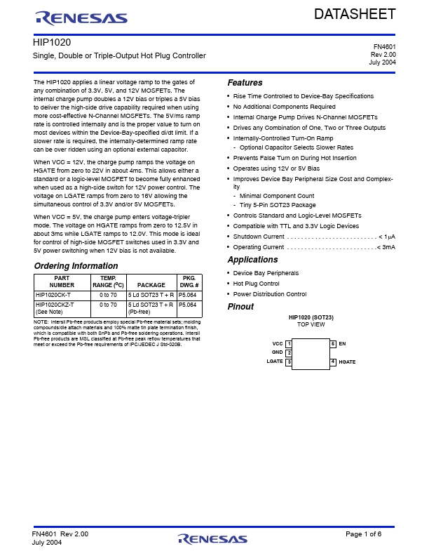
HIP1020
HIP1020 is Hot Plug Controller manufactured by Renesas.
Single, Double or Triple-Output Hot Plug Controller
The HIP1020 applies a linear voltage ramp to the gates of any bination of 3.3V, 5V, and 12V MOSFETs. The internal charge pump doubles a 12V bias or triples a 5V bias to deliver the high-side drive capability required when using more cost-effective N-Channel MOSFETs. The 5V/ms ramp rate is controlled internally and is the proper value to turn on most devices within the Device-Bay-specified di/dt limit. If a slower rate is required, the internally-determined ramp rate can be over ridden using an optional external capacitor.
When VCC = 12V, the charge pump ramps the voltage on HGATE from zero to 22V in about 4ms. This allows either a standard or a logic-level MOSFET to bee fully enhanced when used as a high-side switch for 12V power control. The voltage on LGATE ramps from zero to 16V allowing the simultaneous control of 3.3V and/or 5V MOSFETs.
When VCC = 5V, the charge pump enters voltage-tripler mode. The voltage on HGATE ramps from zero to 12.5V in about 3ms while LGATE ramps to 12.0V. This mode is ideal for control of high-side MOSFET switches used in 3.3V and 5V power switching when 12V bias is not available.
Ordering Information
PART NUMBER
TEMP. RANGE (o C)
PACKAGE
PKG. DWG. #
HIP1020CK-T
0 to 70 5 Ld SOT23 T + R P5.064
HIP1020CKZ-T (See Note)
0 to 70
5 Ld SOT23 T + R P5.064 (Pb-free)
NOTE: Intersil Pb-free products employ special Pb-free material sets; molding pounds/die attach materials and 100% matte tin plate termination finish, which is patible with both Sn Pb and Pb-free soldering operations. Intersil Pb-free products are MSL classified at Pb-free peak reflow temperatures that meet or exceed the Pb-free requirements of IPC/JEDEC J Std-020B.
FN4601 Rev 2.00 July 2004
Features
- Rise Time Controlled to Device-Bay Specifications
- No Additional ponents Required
- Internal Charge Pump Drives N-Channel MOSFETs
- Drives any bination of One, Two or Three...