Datasheet Summary
2:1 Differential-to-LVDS Multiplexer
General Description
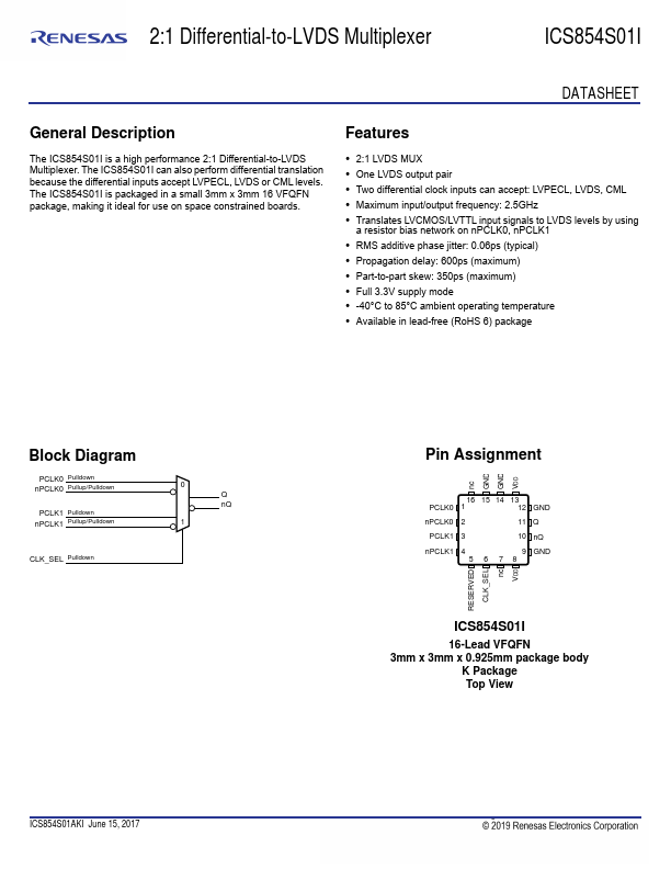
The ICS854S01I is a high performance 2:1 Differential-to-LVDS Multiplexer. The ICS854S01I can also perform differential translation because the differential inputs accept LVPECL, LVDS or CML levels. The ICS854S01I is packaged in a small 3mm x 3mm 16 VFQFN package, making it ideal for use on space constrained boards.
Features
- 2:1 LVDS MUX
- One LVDS output pair
- Two differential clock inputs can accept: LVPECL, LVDS, CML
- Maximum input/output frequency: 2.5GHz
- Translates LVCMOS/LVTTL input signals to LVDS levels by using a resistor bias network on nPCLK0, nPCLK1
- RMS additive phase jitter: 0.06ps...