ICS859S0212I Overview
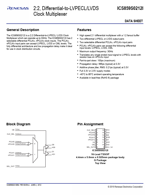
The ICS859S0212I is a 2:2 Differential-to-LVPECL/ LVDS Clock Multiplexer which can operate up to 3GHz. The ICS859S0212I has 2 selectable differential PCLKx, nPCLKx clock inputs. The PCLKx, nPCLKx input pairs can accept LVPECL, LVDS or CML levels.
ICS859S0212I Key Features
- High speed 2:1 differential multiplexer with a 1:2 fanout buffer
- Two differential LVPECL or LVDS output pairs
- Two selectable differential PCLKx, nPCLKx input pairs
- PCLKx, nPCLKx pairs can accept the following differential
- Maximum output frequency: 3GHz
- Part-to-part skew: 100ps (maximum)
- Propagation delay: 565ps (typical) at 3.3V
- Additive phase jitter, RMS: 0.21ps (typical) at 3.3V
- Full 3.3V or 2.5V supply modes
- 40°C to 85°C ambient operating temperature