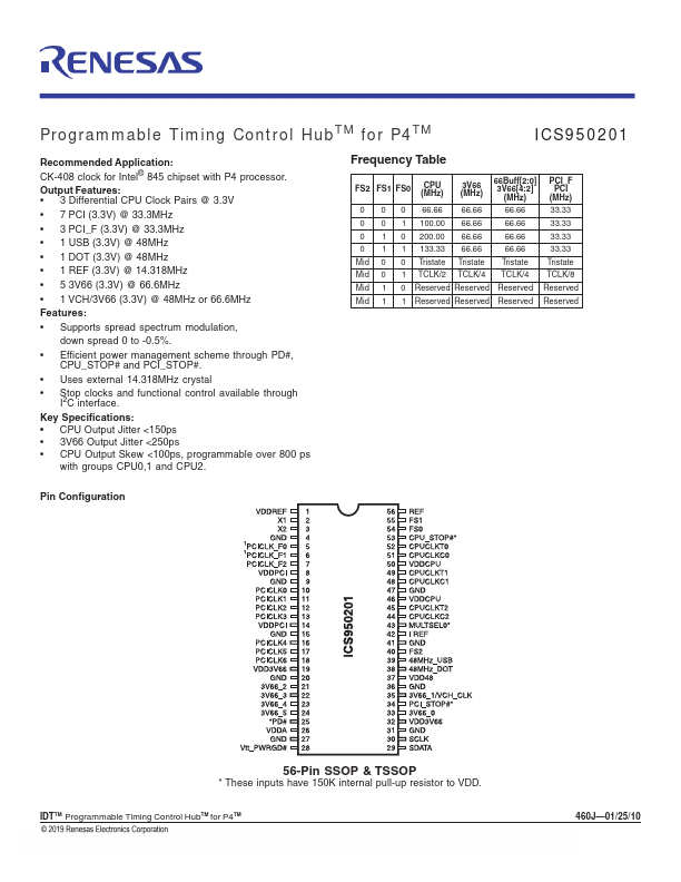
ICS950201
Key Features
- 3 Differential CPU Clock Pairs @ 3.3V
- 7 PCI (3.3V) @ 33.3MHz
- 3 PCI_F (3.3V) @ 33.3MHz
- 1 USB (3.3V) @ 48MHz
- 1 DOT (3.3V) @ 48MHz
- 1 REF (3.3V) @ 14.318MHz
- 5 3V66 (3.3V) @ 66.6MHz
- 1 VCH/3V66 (3.3V) @ 48MHz or 66.6MHz Features:
- Supports spread spectrum modulation, down spread 0 to -0.5%.
- Efficient power management scheme through PD#, CPU_STOP# and PCI_STOP#.